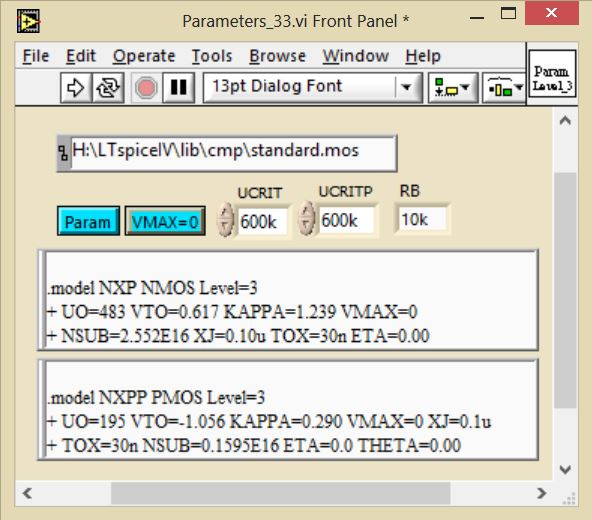
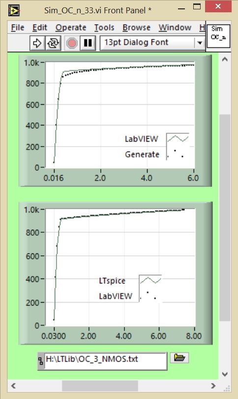
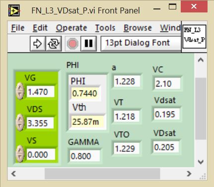
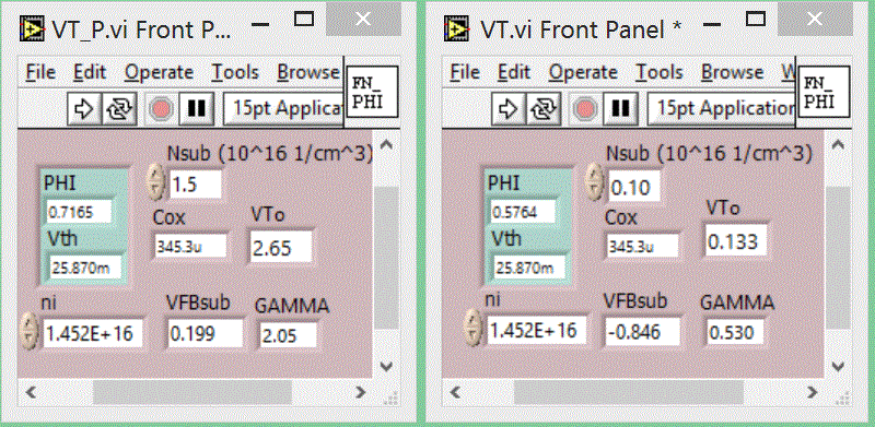
The analysis is based on our LabVIEW circuit simulator, which uses the EKV formulation. The parameters are obtained from curve fitting to PMOS and NMOS devices from the HEF4007US, information of which is available from the NXP logo in the right column. Gate widths for the various devices are based on mP and mM units, and mP=1 is 200u and mN=1 is 100u. The individual m units are selected for the desired current density, and are related to the EKV dimensionless current value, if, for example. (Reference in right column.)
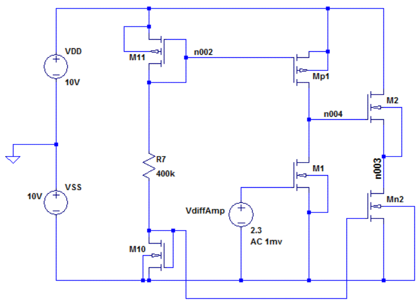
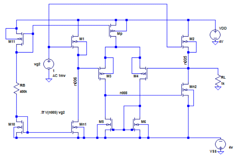
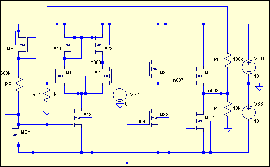
Details are from the following: TS271. The version is created here, and reflects in general the core design of the OpAmp. The circuit is as follows. From input to output, the PMOS and NMOS reference-voltage circuit, the NMOS load differential amp circuit, the PMOS-load common-source stage and the output stage. The latter is a source follower except a special version, which includes a differential amplifier for providing feedback to the gate of the SF load (T16), such as to minimized the change of drain current in T15. A constant VGS15 (with changing drain current) represents a unity gain source-follower stage.

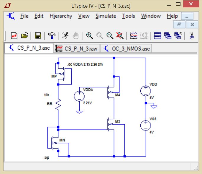
For simplicity, the reference circuit is the standard version, as in the following from LTspice. Similarly, initially, the source-follower stage is the basic version as given here, for comparison. Thus, it is the equivalent to eliminating all transistors beyond T8 and T9 above.
This amp has the opposite (PMOS and NMOS) differential and common-source stages.

Gates
Reference circuit, mP=mM=1.
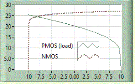
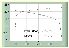
DiffAmp, mP, mN=0.5, ID=25 uA.
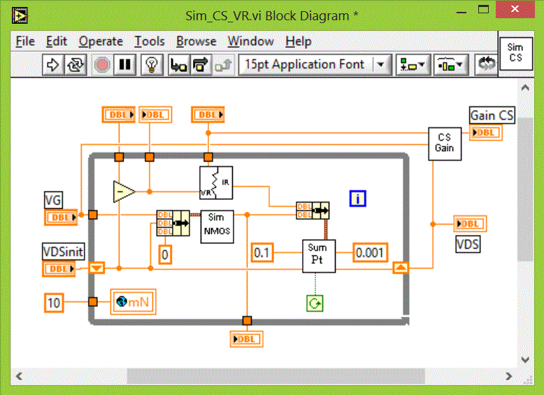
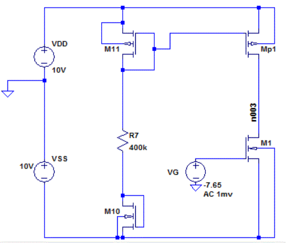
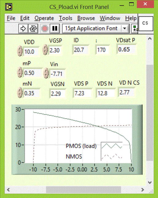
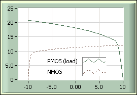
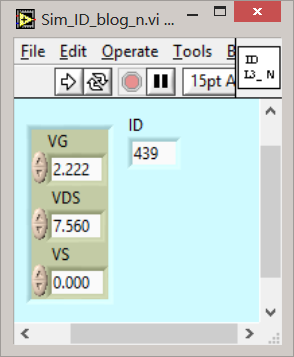
Common-source, m(T6)=0.5, m(T7)=1, ID=50 uA (reference value).
Our simulator uses this balancing circuit: TS271

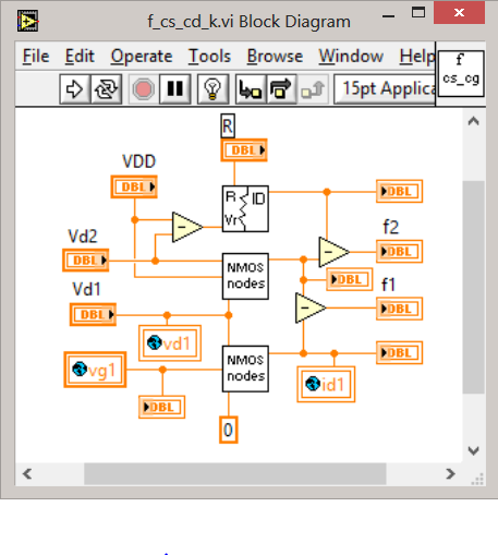
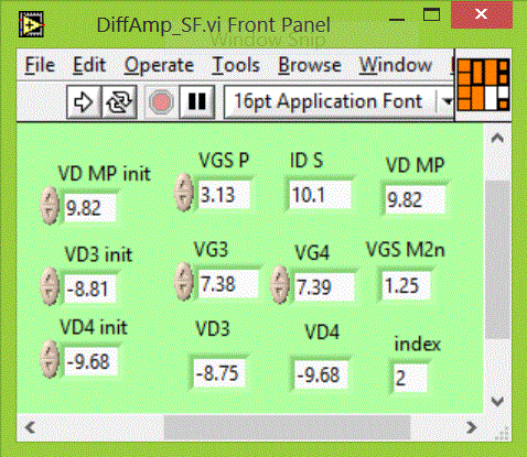
Differential Stage Simulator
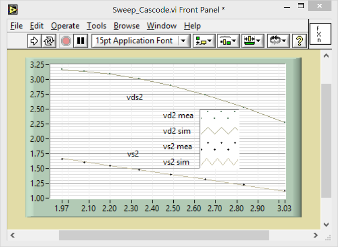
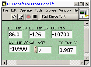
VD2<VD1 due to balance. The potentiometer is set to 0.437 (0 to 1).

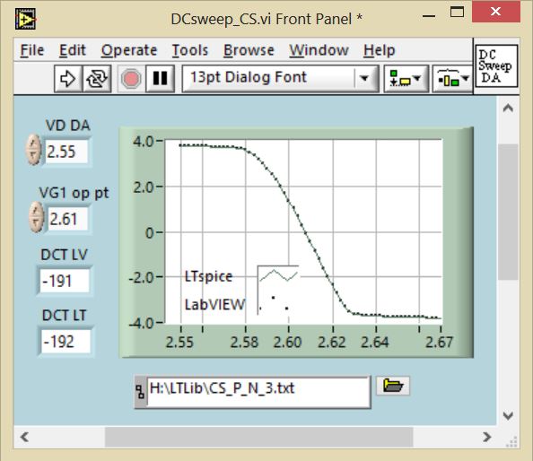
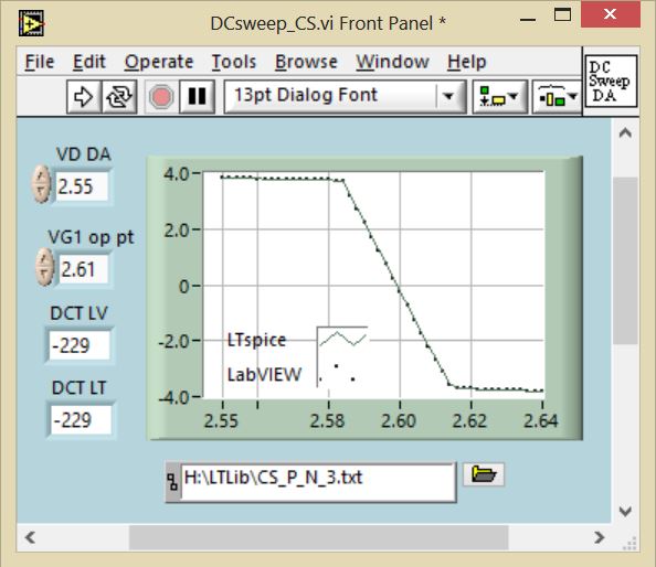
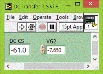
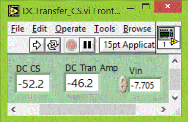
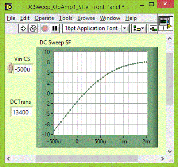
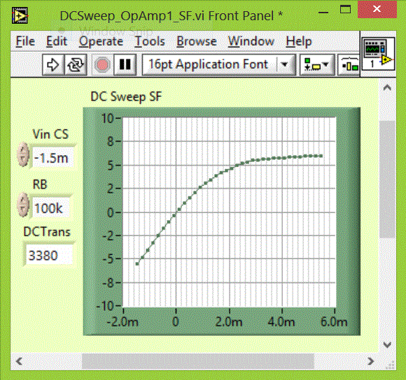
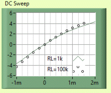
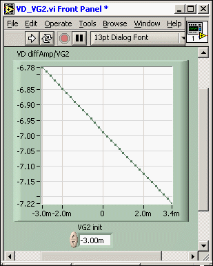
DCtransfer

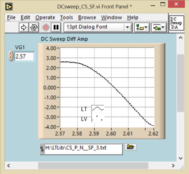
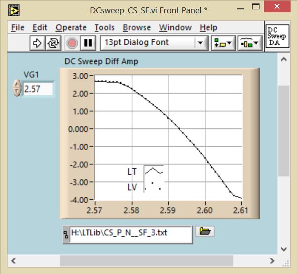
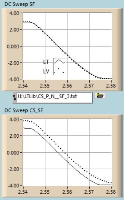
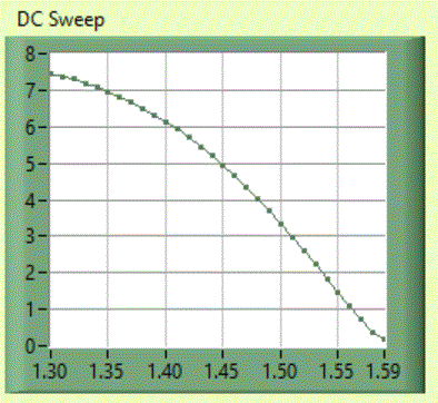
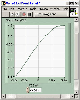
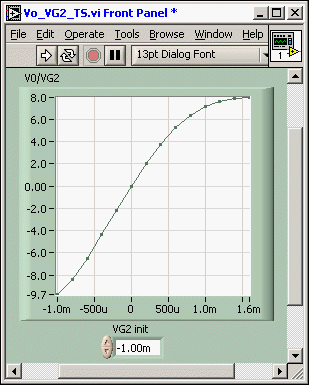
DC sweep

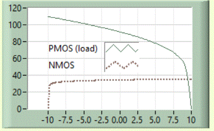
Source follower at max in above plot. Approximately ID (RL)=8 mA.

Negative output.

Negative output with TS271 version of source follower. Note that VGS has dropped only to 1.64 V and the source-follower NMOS current down to 8 mA.

Zero output. VGS=1.76, for transfer ratio (negative) of 0.93. The simple case gives 0.83.

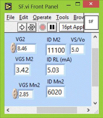
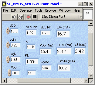
Comparison for positive output. Top: simple SF, ID SF NMOS = 23.3 mA, increasing from 15.6 for zero output. In plot below (TS271 stage), ID SF NMOS increases to only 16.7 at the given output voltage.


DC transfer over a wide range, top, standard SF, bottom, TS271. Smaller DC transfer overall reflects the non-linear output of the open-circuit amp.


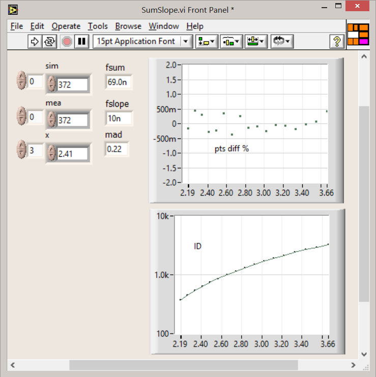


 Slope For For KAPPA – Saturation