Kla's Blog

September 6, 2017

MOSFET SPICE Level 1 Circuit Simulation – PSpice/LTspice/LabVIEW – Design of Opamp Frequency Response – Part 3

Filed under: MOSFET Models — kla @ 3:40 pm

Project Circuit


Gate length L = 2 um. The effects from Cc, Rb and m (m1 and m2) are investigated. Design compensating capacitor is initially Cc = 5 pF. Load CL = 10 pF. Level 1 parameters follow.

Small-Signal Model

Phase-Margin Computer

Parameter inputs include Rbias and m1, m2 gate width. Gate width for this case is W = 5 um (0.05 x 100 um). Computer finds frequency at av = 1 along with phase.

PM Computer Root Finder

Program av sub finds abdb = 0 (Decibels).

DC opamp simulator. Computes all DC info including that for gm, gds and small-signal low freq gains. Has inputs Rbias and m.

Pole – Zero Computer


Plots of characteristics.

Vary Rbias from 30 to 100 k. Plot versus Ids of ms (diffamp current source).

Vary gate width of diff amp m1 and m2 (gm).


Sample Response Plot – W1 = W2 = 5 um.

PSpice Schematics and LabVIEW


September 5, 2017

MOSFET SPICE Level 1 Circuit Simulation – PSpice/LTspice/LabVIEW – Opamp Frequency Response – Part 2

Filed under: MOSFET Models — kla @ 8:15 pm

The Project Opamp

Power supplies, vdd=2.5 V and vss=-2.5 V, are from a sub-circuit. Compensating resistor Rc is initially zero.

DC Simulation with LabVIEW

Common-Source Stage, which dominates the frequency response of the opamp. Resistor rg is the small-signal output resistance of the diffamp stage.

Small-signal Circuit – Cc, Rc = 0

Compute Capacitance – Spice parameters cgso and cgdo. With an applied Cc, the intrinsic NMOS capacitance (Cgd) is added to the total. When Rc is non-zero, the gate-drain intrinsic value is neglected. The junction capacitance (Spice CJ, CJSW) is neglected (for example at the output drains) as it is expected that the external capacitance (at vo) will be large by comparison.

Frequency Transfer Function – Rc = 0 – Below, Rc not zero, with altered zero and additional pole wp3.

With all poles. Pole 3 is made arbitrarily large for Rc = 0.

Phase – Rc not zero.

Level 1 parameters, with capacitance parameters cgso and cgdo for NMOS. Capacitance at PMOS drain is neglected.

(Ref: Allen and Holberg, CMOS Analog Circuit Design, 2nd Edition. Oxford. Chap 3.)


Amplitude and Phase Plot – Include Feedback Factor, B = 1/10, with ideal feedback-amp gain of 10 (20 dB) as in mag plot. Find phase margin PM from phase plot as from curve fits. Cc and C2 = 0. Gain = 100 from diffamp stage is included, i.e., output is referred to Vin.

Pole-Zero computer. Indicated are intrinsic C1 and Cgd use here with SPICE Level 1.

Install C2 = 5 p at output.

Phase Margin drops to a low value with f2 decrease.

PM Root-Finder Computer


Signal circuit with Rc, Cc. Rc initially zero.

Pole, Zero computer.


Cc = 2 pF       C2 = 5 pF

PM

Phase Margin versus Cc. This sweeps the PM Computer, above.

PSpice and LabVIEW Example – Cc = 2 pF, C2 = 1 pF.

Compensation with Rc

Compute Rc for setting the zero equal to pole Wp2. With Rc non-zero, the intrinsic Cgd is neglected.

Plot PM versus Cc.

Rc Compute – Cc and C2 assigned.

LabVIEW and LTspice


August 23, 2017

MOSFET SPICE Level 1 Circuit Simulation – LTspice/MathCAD – Opamp Frequency Response – Part 1

Filed under: MOSFET Models — kla @ 6:02 pm

The project Opamp. Cascade of a diffamp, common-source, and source-follower stages. The power supply is from a sub-circuit and is plus and minus 2.5 V. Id (ms) and Id(m6, m7) are about 200 uA.

The Common-Source stage, which dominates frequency response. Gate resistor Rg is the output resistance of the diffamp stage. at the drains of m2 and m4..

Initially,  the capacitance of Level 1 LTspice (or PSpice Schematics) is matched with MathCAD for the case of a single pole, based on C1. Cc=Cgd  and C2 are for now made zero. Gate resistor Rg is the output resistance from the Diffamp stage. R2 is the combined  output resistance from m6 and m7. CL = C2 = 0.

Signal Circuit

MathCAD: Compute circuit current, Id.


Compute g Parameters. (Diffamp parameters computed elsewhere).


Compute C1, consistent with LTspice and PSpice. Assign a value to SPICE parameter cgso.  The first term in C1 is LTspice Level 1 default.

Plot common-source stage small-signal voltage gain versus frequency.

Phase Plot

LTspice

Include capacitor Cgd with parameter cgdo. This is Cc equivalent to the Opamp above, except internal to the NMOS, in this case. Make C2 = 1pF.

The gate-to-drain capacitor produces an additional pole and a zero, as computed here, which adds to phase shift. Also, the effective capacitor value is enhanced by the Miller effect.

Frequency Plot

LTspice


May 1, 2017

LabVIEW MOSFET Simulation Model Generation by Curve Fit – Part II

Filed under: MOSFET Models — kla @ 4:35 pm

Part I

A best match is obtained between Level 3 and EKV MOSFET circuit simulators, even though the model parameters are somewhat artificial. These three examples illustrate some possibilities. The Level 3 simulations are confirmed with LabVIEW, PSpice Schematics and LTspice. EKV is matched between LabVIEW and LTspice. All three are the result of curve fitting as discussed in Part I. The best fit is around 2.5 V, which is the drain voltage of variable vg plots that are used in curve fitting. The full range  is that of the range of the power  supply magnitude.

UCRIT = 2 meg VMAX = 40 k

UCRIT = 2 meg   VMAX = 0

UCRIT = 10 meg   VMAX = 0

The last example will be used here for some curve-fitting exercises, although the UCRIT value is large. A DCsweep is performed on the following circuit for the two simulators.

The Pars 3 ICON (left) performs a curve fit to EKV-generated plots to obtain Level 3 model parameters on each run.

The Write ICON sends a .txt file to be read for comparison.

This program receives Plot Data (such as above DCsweep) or that from three arrays (top) and is sent according to the file path and name.

Level 3 and EKV compared with .txt files that are read.

Array Subsets are included to, for example, eliminate a title line in the data.

DC Transfer

Basic Op Amp

DC Sweep – UCRIT = 5 meg – VMAX = 0

UCRIT = 2 meg

UCRIT = 2 meg   –   VMAXn = 50 k, VMAXp = 20 k

OC curve fit, NMOS

OC curve fit, PMOS

Sat region KAPPA curve fit, NMOS

VMAX = 0

April 28, 2017

LabVIEW MOSFET Simulation Model Generation by Curve Fit

Filed under: MOSFET Models — kla @ 8:54 pm

Part I

For the equivalent of data as would be obtained from chip measurements, data are generated using the EKV simulator with the goal of obtaining Level 3 simulator model parameters. An example follows, based on the LabVIEW simulator. These plots could also be obtained, for example, from LTspice.


The plot is saved as a Cluster Global Variable, as shown.

Data vi

Here is a curve-fitting simulation computer with an example input from the data. This is for UO, and since parameter vb depends on UO, it must be updated with UO as shown.

NMOS Parameter Extractor

The three iteration files are in series in a loop. The Loop halts when the change of UO is small as set as 100 u. 

UO

Iteration – Variable vx is a generalization and is UO in this example. Loop runs until deltaUO (per loop) is less than 1 u.

Iteration function. Function f sum value is the mean difference between points, relative.

Global Variables UO and vb (Level 3 parameter) are contained in ICON UO vb. Level 3 simulator in the Loop uses these variables from Global Variables. Loop runs for all index values. Two plots are compared lower, right (above plots).

Sum – Slope

UO uses f sum, and halts for an assigned minimum value. The sum is the mean of the relative difference of points, thus relative to one. The indicator in the plot is the difference in drain currents, mean. The fact that this is not a constant value versus vg is an indication of a difference between Level 3 and EKV.

The slope function  is a LabVIEW straight-line curve fit to the difference of the two plots, ekv and Level 3 in this example.

VTO Function – Slope Fit

KAPPA – Slope Fit

Index for the beginning of the saturation region is computed as shown here.

Complete OC simulation. NMOS.

PMOS

Parameters

VMAX, TOX, NSUB and THETA  are assigned. ETA = 0 gives the best fit.

April 26, 2017

MOSFET Level 3 Spice MOSFET Circuit Simulation with LabVIEW and LTspice – Part II

Filed under: MOSFET Models — kla @ 7:22 pm

Follows Part I

Level 3 Simulator Detail

Create Global Variable VI with basic physical parameters. These are assigned and computed for 27 C. Go to (EKV) v262 in right column for example of temperature dependence.

Assign parameters and compute parameters based on NSUB.

All parameters are sent to simulator as Global Variables.

Parameters Set

NMOS Basic Level 3 Simulator (VMAX = 0, i.e., no carrier velocity saturation is included).

MOSFET Level 3 Spice MOSFET Circuit Simulation with LabVIEW and LTspice – Part I

Filed under: MOSFET Models — kla @ 2:12 pm

Common-Source Gain Stage

Newton-Raphson Root Finder – Two branches with one node. Find vgn and vo.

Iteration  Function

Reference voltage circuit. NMOS has 0.5 x standard width and uses circuit node connections.

Performs node-pair conversion according to Level 3. This version is for no body effect, with Vs =0.

Basic node-pair Level 3 NMOS simulator.

Circuit Simulation

Reference voltage vgn simulator.

Iteration function currents and f plotter.

Common-Source

Common-source f diagram. Iteration voltage, vo.

Convergence

Circuit Simulator

Includes signal-gain computer, av = 88 above.

Current and f plotter with vo sweep minus to plus power supplies.

July 26, 2016

LabVIEW Newton-Raphson MOSFET Circuit Simulation

Filed under: MOSFET Models — kla @ 2:55 pm

The first project circuit is, as shown, a reference-voltage circuit, Vgp. The iteration function is f = Id (pmos) – I (Rb), with f = 0 at the solution. The LabVIEW simulator is below. The PMOS simulator here is Level 3 Spice.

circuitf_LV

The function f plotted against the iteration voltage v, with solution v =Vgp at f = 0.

f_plot

First iteration step.

st_line_plot

Generation of the plot. Loop on the right finds the plot index for f at sign change, and the index is used to obtain an approximate value of Vgp, as indicated above. Index is 7971 of 10000. Array v is the input to Index Array with Vgp output.

rootf_BD

Generate First Step

st_line_plot_BD

LabVIEW Iterator Program with solution, for init value v = 2 V as in the above plot.

iteration_2V

Init value v = 3.6 V

iteration_3.6

Init value v = 3.8 (> solution). The indicated f is the final difference between the two currents.

iteration_3.8

Iteration Program. Voltage v inputs to f  function are v + v/100k and v – v/100k. The small difference provides for an incremental f, df, to form the derivative for a known dv.

iteration_BD

Iterate –

iterate

iterate_BD

PR % = 0.0001

iterate_2

Capture


March 31, 2016

LTspice Sub_Circuits Illustrating Cascode-Circuit Effect – EKV Simulator

Filed under: MOSFET Models — kla @ 6:53 pm

The supply and reference voltages for this project are as follows for all circuits evaluated here. This provides for a variety of circuit configurations.

vref

The following sub-circuits are created for the supply and references.

Capture

The supply voltages are for this case internal to the sub-circuit.

Capture

The library files are located as shown.

Capture

A simulation of the above circuit produces the net file, as shown, from which the reference-circuit file can be copied.

Capture

Basic Amp – Fig. 1

1.) Symmetrical Diff amp input stage, 2.) single-ended diffamp gain and output-stage adapter, 3.) output stage. Diffamp output voltage should be about zero for minimizing common-mode input to the following single-ended output diffamps but slightly positive vp and vn improves the performance of m1 and m2.

Capture

With sub-circuits.

X2 calls power-supply voltages, X4 calls reference voltages, both in vref.lib.

Capture

Subckt example. Symmetrical Diffamp sub-circuit. Label input and output nodes, vg1, vg2, von, and vop, (F4). Simulate and obtain net file (below).

Capture

Capture

Create dansym subckt.Capture

From LTspice, lib, sym, opamps, open opamp2, for example.

Capture

Edit for this application and name and save.

Capture

When creating the above circuit with subckts, use F2 for opamps, and place the subckt symbol.

Do a right mouse, and bring up this window and enter value (subckt name).

Capture

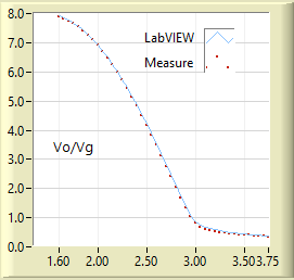
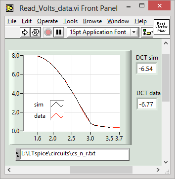
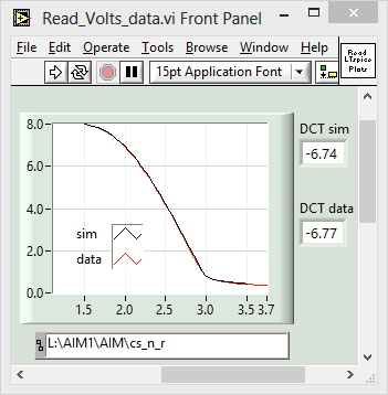
Perform DCsweep (Fig. 1). In this case, we read the LTspice file with LabVIEW and compute the DCtransfer.

Capture

MOSFET Parameters (EKV)  generated by LabVIEW for given NSUB, etc.

Capture

Symmetrical diffamp with common-mode feedback circuit (right).

This version includes CMFB circuit for holding  outputs (vp and vn) near zero. Note that ms2 and ms3 are not necessarily required and that m5 and m6 are diode-connected PMOS devices.

Capture

With Subckt CMFB and subckt reference voltages and power supply.

Capture

Capture

PMOS Current-Source Diffamp. We note here, that with vo = 0 V, Vds of m1 and m2 is small.

Capture

DCtransfer

Capture

Add common-gates, m5 and m6.

Capture

DCtransfer – Output resistsance dominated by rds of m1 and m2.

Capture

Folded cascode load. m9, m10, m7, and m8 are in the common-gate mode. In this circuit, the common-gate devices have large source-degeneration resistance.

Capture

Capture

Opamps with Common-Source Gain Stage

Basic

Capture

Capture

Add cascode NMOS

Capture

Capture

Add PMOS Cascode

Capture

Capture

November 7, 2015

LabVIEW Spice Level 3 Simulation Exercise

Filed under: MOSFET Models — kla @ 7:26 pm

In this project, we obtain Level 3 SPICE simulation parameters from measured data of our device, and apply them to the following basic circuit. Level 3 variations are given extensive considerations.

DCsweep, Transfer Characteristics, and Output Characteristics measurements are made on our project circuit, which follows. Rb is made a smaller value for Xfer and Output characteristics, for example about 1k.

circuit

NMOS is from this chip, pins 6, 7, and 8.

chip

Measured data are stored as Global Variables.

dataGlobal

Parameters – Extraction always uses the Level 3 Version as to be applied. The 1 selection applies to the simulation step shown just below. It selects by way of the Global Variable sw (binary) K= 1 or K=KAPPA, for AIM spice or LTspice, respectively, for the Ep form. (PSpice uses KAPPA.) The button param when selected to binary 1 sends a parameter file for the simulators. Upper UCRIT vales are for K = KAPPA, lower values are selected for K = 1.

curvefit

Capture

Ep is used in the final Level 3 simulator stage. An alternative is to assign Ep according to other uses, including Ep = 0.

Capture

Curve fit to xfer characteristic X, for UO, sum. Slope fit finds VTO.

Capture

Slope fit to oc, sat region, finds KAPPA.

Capture

Sample NMOS Parameters – This runs under N_P_pars.vi above.

Capture

Measured amp data, Global Variable, DCSweep, sample.

Capture

DCsweep with Level 3 simulation. Note that Data oc is approximately mid range to the application range. Here, the LabVIEW simulator uses Ep = 0 (lc = 0) or Ep = Vdsat/Leff, with similar results. This is equivalent to basic Level 3 (VMAX = 0) for the output (channel-length modulation) but here, the effect of velocity-saturation effect is still present.
CaptureCapture

Following are Simulations comparing LabVIEW with AIM spice and LTspice, based on their respective versions of Level 3 SPICE. The simulators are discussed, for example, here. In the above LabVIEW simulation, Ep = Vdsat/Leff.

aim_lvlt_lv

Compare simulation, LTspice, with data, and AIM spice with data.

lt_dataaim_data

Older Posts »

Create a free website or blog at WordPress.com.