K.L. Ashley
Analog Electronics with LabVIEW
The Level 3 Spice model used here is described in the following. (In the Process of additions.)
A goal here is to demonstrate that the above model documentation is valid insofar as simulations fit precisely the simulations with LTspiceIV. LTspice Level 3 and Schematics (Microsim/OrCAD) are essentially identical. Simulation matches appear to call for a slightly altered value for the relative permittivity of silicon, and the choice of value has changed slightly over time.
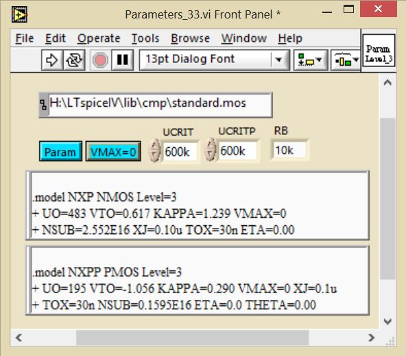
Parameters: UO, VTO, KAPPA, NSUB, VMAX, THETA, XJ, RS, RD, and ETA.
Synthetic measured data – equivalent are generated with a precision simulator. An example is shown here. TOX, GAMMA, UCRIT, and VFB are selected to create the model functions. The example plotted here is for a P-well, tox = 100n, with this being the NMOS. Some numbers are below in the VI NMOS_Par_init. VFB is adjusted to simulate an implant. VTO and UO are obtained with a fit to the Xfer function (left plot, ID uA and VG) characteristic and KAPPA from the OC (ID uA, and VDS). TOX = 30 n. The drain-current magnitude suits the Level 3 model except for the OC pre-sat, but it is not used for curve fits. (N-well with implant reviewed below.)


An example curve fit (above plot) top, and simulator comparison follows. VMAX = 0.
Curve Fit Program
UCRIT is set essentially to infinity for VMAX = 0. The values shown are examples for the case of VMAX not zero.
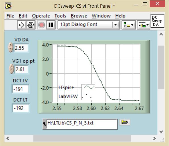
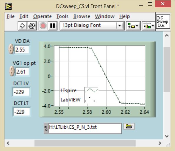
DC Sweep of Common-Source Amp Stage -LabVIEW and LTspice
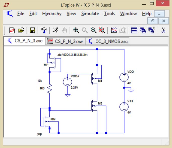
 Circuit
 VMAX non zero with LabVIEW and VMAX = 0 for LTspice

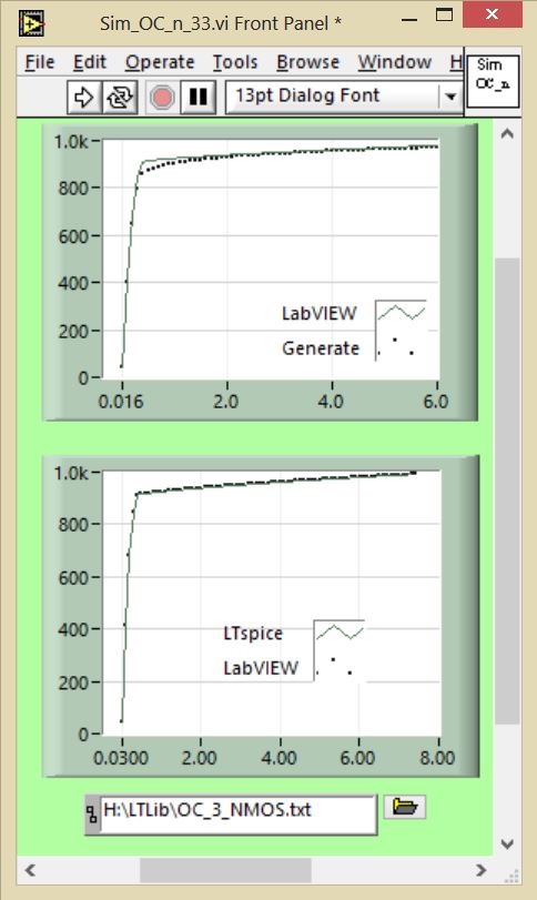
OC
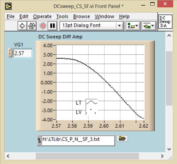
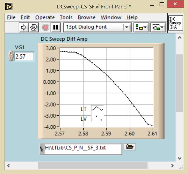
 CS plus Source-Follower – LabVIEW
 VMAX non – Zero

N-well
The Level 3 parameters are now as indicated here. An implant of Vd = 0.5 V is included, to increase VTO of the NMOS and decrease that of the PMOS. Parameter is now tox = 30 n.

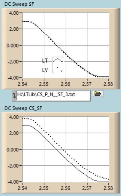
DCsweep – Top – LTspice and LabVIEW – Bottom – Common Source and Source follower
Voltage drop across SF M1 is reduced from above case. The gate width of SF MOSFETS is 10 times that of the CS. The load is 4 k Ohms and thus max load current is about 1 mA and minimum voltage out. The drain current must be set equal to zero at some point for negative voltage out for M1 since Level 3 is not valid for very low currents.
 DC sweep of CS Stage – VMAX zero and VMAX non-zero
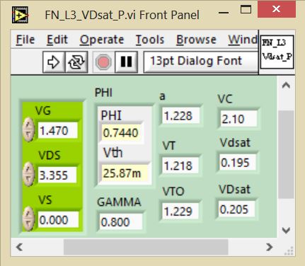
 LabVIEW Simulator Sub – VMAX = 0 VDsat = Vdsat (velocity saturation effect)
 VMAX non- zero – Vdsat is 10 mV less that VDsat (VMAX zero)