Kla's Blog

February 28, 2013

EKV and Iteration MOSFET Model

Filed under: Uncategorized — kla @ 11:09 pm

This model is the EKV equivalent, with respect to depletion-region charge gate-voltage approximation.

Model

ekvpaper1

ekv_v262

Page 179

PSPICE

Model (VFB  is minus)

Capture

EKV

Captur2

X1 Curve fit comparison.

Alles

Iteration VI  – Typical index is 1 or 2.

Capture

Alles

Common Source Amp simulation  with RD=47k, DCsweep.

Alles

February 25, 2013

LabVIEW MOSFET Parameter File Construction

Filed under: Uncategorized — kla @ 11:37 pm

The File Creator

Capture

File Assembler

Capture

Capture

String Functions

Capture

Extractors and Links to Global Variables

Capture

Sample Global VI which stores Parameters

CaptureParameter Connections in NMOS Extractor

Capture

February 21, 2013

MOSFET Operational Amplifier with Feedback

Filed under: Uncategorized — kla @ 11:21 pm

Op Amp with open circuit: Output (VS SF) is -400mV.

Capture

Adjust VG2 for approximate zero out. DC transfer is 400/mV/104uV=3800 (non-inverting).

Capture

Op Amp with negative feedback. Output is approximately zero, i.e., VG1 approximately 100uA (from above), and VS SF is approximately 100xVG1=10mV. Note that from VG2, the amp is non-inverting: A cascade of Common Source (inv), Common Source (inv), and Source Follower. With VG1 input: A cascade of Source Follower, Common Gate, Common Source (inv), and Source Follower.

Capture

Feedback Amp simulator. DC transfer (inverting) is (400mV – 10mV)/100uV or  about 3900.

Capture

DC transfer simulator.VG1 is plus and minus 60 mV=120mV. Input feedback (VG1) is 116.7uA for net gate increment of 3.344uV for an internal DCtransfer of 3520k. Amp gain is 98.2, which is dVout/120mV.

Capture

Summary

Capture

Comparing DC transfer with open circuit and that biased to zero out. Top: Zero DC gate voltage, Vo=-0.4V, Bottom, VG1 biased for zero out. Open circuit gain is a function of DC bias as gain depends on the variable slopes of the MOSFETS in saturation.

CaptureCapture

February 20, 2013

LabVIEW MOSFET Operational Amplifier Simulator

Filed under: Uncategorized — kla @ 7:19 pm

Complete simulator with DC transfers at each stage, RD=100k.

Capture

RD=10k

Capture

Current-Source Voltage

Capture

Capture

Simulator: Halts on current match.

Capture

Example

Capture

Current Source

Capture

Result for grounded drain.

Capture

Differential Amplifier

Capture

Simulator

Capture

PMOS-Diode NMOS

Capture

PMOS-NMOSCapture2

Result

Capture

LTspice DC output.

Capture

CS Stage

Capture

Simulator: Gate widths of M7 and M8 are in the ratio of 2:1.

Capture

Simulator Results

Capture

OpAmp: Gate width of M9 is 5x the standard.

Capture

Source-Follower

Capture

Capture

Op Amp

Capture

DC Transfer

Capture

Op Amp Two

Capture

DC Transfer

Capture

February 10, 2013

PMOS Common-Source Source-Follower Amplifier Evaluation with EKV Simulation

Filed under: Uncategorized — kla @ 7:34 pm

Our two-stage amplifier circuit is here from Schematics.

Capture

The PMOS parameter extractor is given here. This is based on LabVIEW 7.0 on Windows 8. The graphics are from Windows 8 application Snipping Tool. As shown below in the plot for finding VFB (VTO), the fit is for a wide range of data. M1 above has ID of about 10uA whereas, M2 has ID on the order of 1 mA. The loop for the parameter is shown below. Note that it is a slope fit, whereas, KP (UO) uses the sum for a fit to these same data.

Capture

Capture

Parameter VFB is iterated to find the best slope fit. It is sent to the initiating FN (formula node) of the simulation, as shown below. This parameter is used directly to compute the parameter VP, which is used to compute the dimensionless drain current with the interpolation function. VTO is not actually used other than as a parameter in the simulator, and it can be used to compute other parameters.

Capture3

Capture

The KP VI is given here, with Block Diagram following.

Capture

Capture

Parameter KP is then used in the final FN, as shown here. The effective L is also computed, which uses UCRIT and LAMBDA.

Capture

Using the LabVIEW simulator, a DC sweep is performed as shown here. A choice for bias VG1 is 1.7V. The bias current for M1 is about 10uA. The DC transfer at the bias voltage is indicated.

Capture

The DC sweep for the source of M2 as the output is below. The gate-width of M2 is made 3 times that of M1 to reduce the VGS2 value, with a DC output at the bias output voltage of about 1.5V and a bias current of 1.5mA, an overall DC transfer of 34.8.

Capture

The DC sweep simulator Block Diagram is here. The ICON on the right is a similar loop for the source-follower. In the first version, the iteration is on VDS1 and halts when the circuit VDS, VDD-ID*RD, is equal to the input VDS to the PMOS simulator. The second version has an input voltage to the resistor and the iteration halts when the current through the resistor is equal to that from the PMOS simulator.

Capture

Capture

A Schematics DC sweep is  here. We note that the output voltage negative with the positive voltage in the circuit at ground in this case The result agrees with LabVIEW with VD1=4V absolute at VG1=1.7V.

Capture

The Schematics DC  transfer is here, and in agreement with the LabVIEW result.

Capture

LTspice gives the following for the same circuit and identical PMOS parameters.

Capture

February 2, 2013

Common-Source Amplifier Measurements with NI NI-DAQmx at Low Drain Current

Filed under: Uncategorized — kla @ 8:58 pm

The Auto Ranging Voltage/Drain-Current measurement was shown in the last article to provide precision measurement at low voltages. Here advantage is taken of this to characterized a common-source amplifier with operation in the range of ID of a few uA. The amplifier is the parameter extraction circuit but with a much larger RD. The circuit is here from LTspice. Note that the operating-point drain current is  about 8uA for VD1=4V. For the wide range of current, including low values, the EKV  simulation model is used.

ALLES

The measured DC sweep is as follows, which also displays the drain current. The measurement functions are originated with DAQ Assist. Drain current is measured with our standard auto-ranging device, although the voltage across the resistor is large. The DC transfer is for VG1=1.41 volts  and VD1=3.98 at ID=8.38uA as shown.

ALLES

ALLES

The parameters are extracted from a very wide range of drain current, as shown here for UO/KP. The data is precision as described in the last article with auto-ranging current measurement.

ALLES

The LabVIEW simulated DC sweep is here, and is noted to be accurate when compared to the measured data. The single-point simulator below gives the DC transfer and the simulated VD1 at the op VG1=1.51V

ALLES

ALLES

The LTspice DC sweep follows (EKV, Level =12).

ALLES

The following is a plot of the DCsweep, including the DCtransfer. This was obtained using LabVIEW 2012 (Student Version) and on Windows 8. For maximum gain, the bias gate voltage is about VG1=1.55, with a signal range of approximately 2V.

P

Auto-Ranging NMOS Drain-Current Measurement with NI NI-DAQmx

Filed under: Uncategorized — kla @ 12:01 am

This is revised for brevity and a new version of the range selector.

This is a follow up to the previous post on measurement. The plot is the drain-current resistor voltage of the transfer characteristic for parameter extraction (Y-axis) versus the gate voltage.  The minimum current is about 1uA. Thus, it would be applied to wide-range models such as EKV. For these devices, the lowest current is associated with weak inversion, as VG<VTO.

With the range of the voltmeter set at the range of -10 to 10V, the drain-current voltage is as follows.

Alles


An expanded scale plot is shown here for comparison with a measurement which automatically sets the range of the measurement according to the magnitude of the measured  voltage. The auto-ranging case has a range of 0 to 100mV.


Alles

A possible two-selection auto ranging is as follows. An initial measurement is made, and true or false is selected for the low and high range, respectively, where the high range is 0 to 10V for all positive voltages.

ALLES

An example of a generalized auto-ranging voltmeter is now considered. The VI for selecting is as follows. Any collection of limits can be installed, with the associated Case. The Block Diagram below shows Case 2 (small voltage) and the selection mechanism.

The initial measurement is made with Vi2, which is set for Vmax=10V. The various range maximums are installed in the Limit array. In this example, 0, 1, and 2 cases are used, with maximums of 10, 1, and 0.1V.  In the example, the test voltage is 32.5 mV with a final measurement of 30.7 mV, for a measurement with a limit of 100mV. The loop index is 3, as a result of looping through the array to find the “less than” condition.

Alles

Alles

A comparison of simple 10V max versus auto-ranging is here. With the 8-bit DAQ and unipolar, the 10V resolution is 10/4096 or about 2.5 mV. We note the variation at the lower level for the 10V (higher) case. The 100mV minimum max range is adequate. The bottom plots are for the simple case but with the range of +10 to -10V, for bipolar.

ALLES

ALLES

February 1, 2013

MOSFET Parameter Extraction Data Obtained with NI NI-DAQmx

Filed under: Uncategorized — kla @ 7:59 pm

The measurements consist of a transfer function with constant VDS and an output characteristic. The DAQ is an E series, and the system is Windows XP, LabVIEW 7.0, with NI-DAQmx 7.2. The circuit from LTspice.

ALLES

From the Block Diagram, Functions is opened, followed by Input/DAQ Assistant.

ALLES

ALLES

DAQ Assistant is opened and Analog Input is selected.

ALLES

Voltage is next selected.

ALLES

Channel ai0 (zero) is selected, and this will be repeated for ai2.

ALLES

In the next step, 0 to 10 V is selected, for the NMOS (all positive), as -10  t0  +10  has half the resolution. 100 samples is picked for averaging. The data rate is not critical.

ALLES

The case is named accordingly, such as the case for a possible ai1.

ALLES

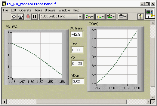
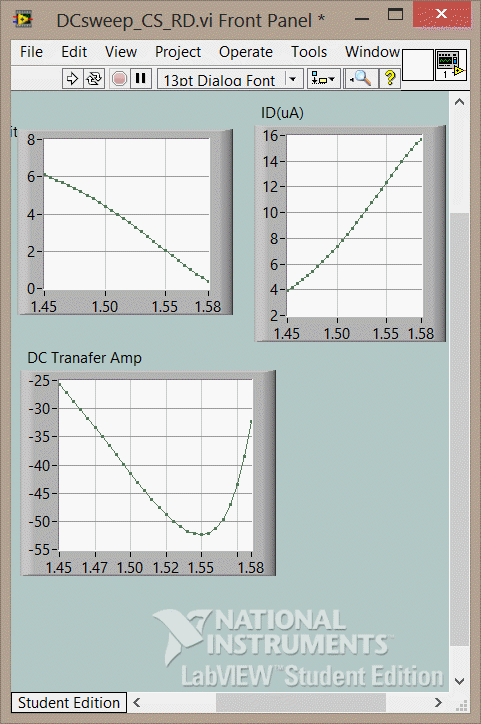
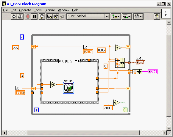
For building the X1 VI, this is repeated for input ai2 and outputs (2). The first step (Frame 1) appears here. VG1 (in Icon form) is assigned the series of voltage, VG1, starting with VG1=2.4 and incremented up in steps of 50mV, in the For Loop.

ALLES

In the next frame, VO loop is executed. This sets the drain voltage at an assigned value for each VG1.

ALLES

The VOloop diagram is as follows. It contains output voltage ao0 (configuration below) and voltmeter VO, which reads the drain voltage (below).

ALLES

ALLES

This voltmeter reads 10 samples and these are averaged as shown. This is not a critical voltage, as MOSFET drain current is insensitive to it.

ALLES

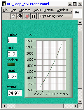
The VOloop Front Panel shows the progress towards establishing the goal VDS. The lower plot has x-axis index, and the case is very over-damped, for effect, as is the poor selection for the initial value. The damping factor is the “1”  just outside and below the loop above.

ALLES

The drain current frame follows. The measurement uses 100 samples, which are averaged, and set for uAmps.

ALLES

An alternative loop is a While Loop, which halts at a given set max drain current.

ALLES

An example X is here

ALLES

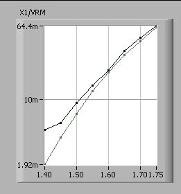
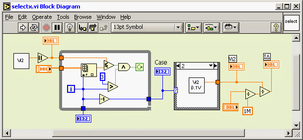
A wide-range example is here. Voltmeter two (drain current, VRM) is reading over 2 orders. The resolution is suspect at the lower end. This is ameliorated with using a LabVIEW case structure to  select an appropriate voltmeter for a given range and could consist of multiples of 2, 5, and 10 and for varies orders of magnitude. For Level 3, this is not required.

ALLES

The measurement system is contained in X1data.vi, with Block below. This preserves the data, such that it can be accessed anytime after the measurement. The “false” state uses Local Variables to preserve the data, as shown 2nd below. The data array is in Global variable XM1.

ALLES

ALLES

ALLES

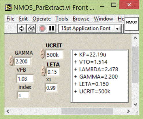
An NMOS parameter structure for our projects is here. As in the Diagram below, the above data are placed in the initial frame of execution.

ALLES

ALLES

For example, the UO loop uses XM1, as shown here.

ALLES

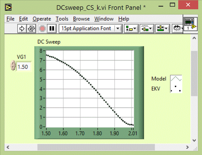
The curve-fit loop is here. Icon X1 N is the data array applied to the simulator, below. The simulator is Level 3, and thus, has a relatively small drain-current range.

ALLES

ALLES

ALLES

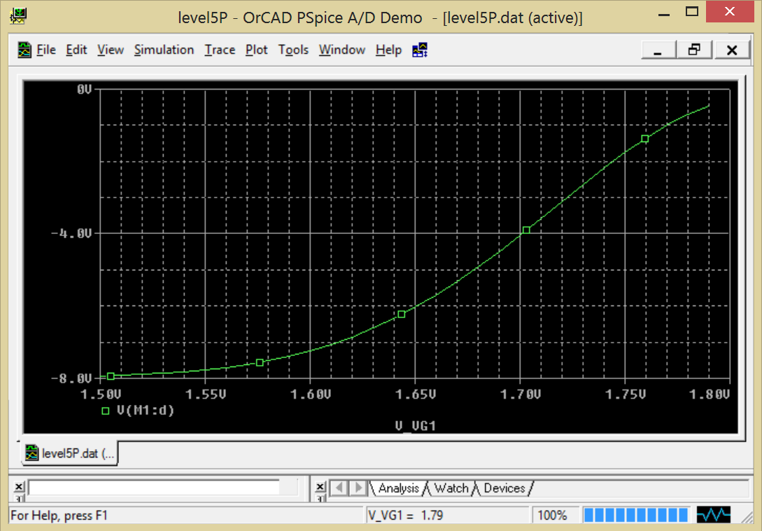
Special considerations for the PMOS, with negative voltages, are required. The measurements could be made with a positive voltage configuration, but this requires that difference of voltages be applied, which gives up lot in precision.  Shown here is a minus gate voltage application. All voltages are converted to positive for  simulation purposes.

ALLES

ALLES

In the VDS loop, a negative voltage (VDD) is applied but the negative input voltage (VDS) is made absolute, such at the same loop execution occurs as with the PMOS.  As below, the voltage range is plus and minus.

ALLES

ALLES

The OC measurement is a simple loop, as shown below. VDD is stepped through a range for a given VG1. The Voltmeter shown includes averaging.

ALLES

ALLES

The OC data has the option of run or store and use.

ALLES

Blog at WordPress.com.