TS271 Output Stage
vg2 is from the common-source stage. Parameters generated here are used as are gate widths.
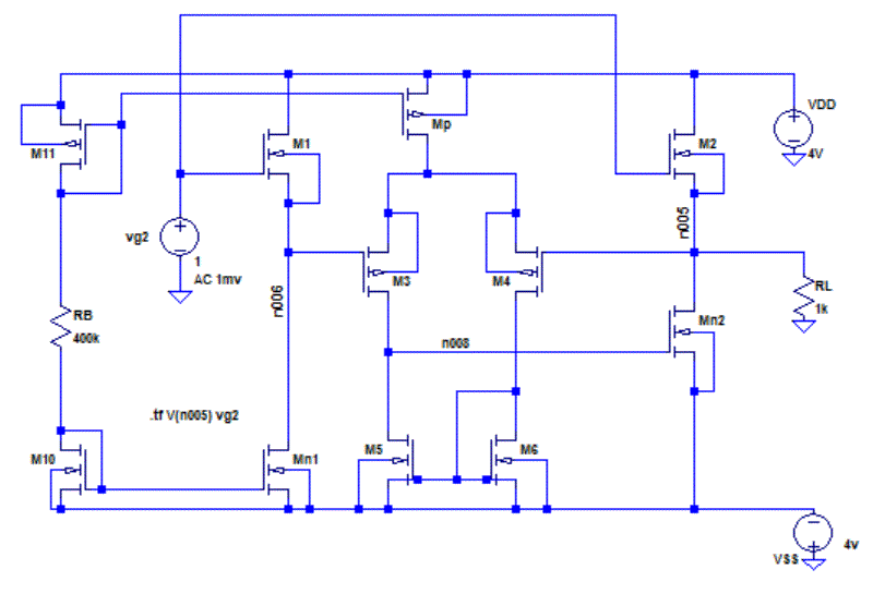
The circuit is here.
DCsweep with LabVIEW simulator (EKV).

Common-Source Output Characteristics at Maximum Above
PMOS load is in pre-saturation. CS output is 9.56 V (vg2 in above circuit).

Output Source-Follower Results at Maximum
VGS M2 (output NMOS above) is 1.66 V. Output is 9.56 – 1.66 V=7.9 V. Case is for a small load current.

Simulator for M5 and M3, Above
Gate of M3 is at 7.89 volts. VGS3 is 1.99 V. Thus, drain of Mp is at 9.88 V, or has reached the limit. This is VD Ms in VI below.

Parameter Generator
Model is based on a P-Well (NMOS) and an implant as given. Nsub given is times 10^16 1/cm^3.

