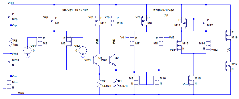
Opamp 1 – DiffAmp stage and common-source stage. Gain stages all have ID = 100 uA. Reference current is 50 uA. NMOS – W = 100 u PMOS – W = 200 u Relative Mrn – 0.5, Ms – 2, M3 – 1.

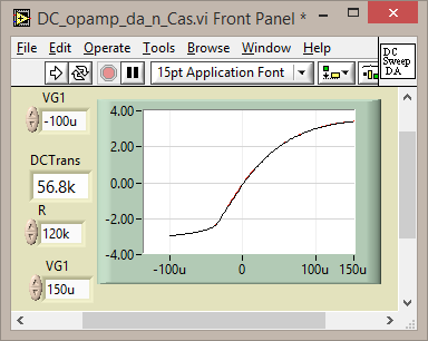
DC Transfer – Diff Amp
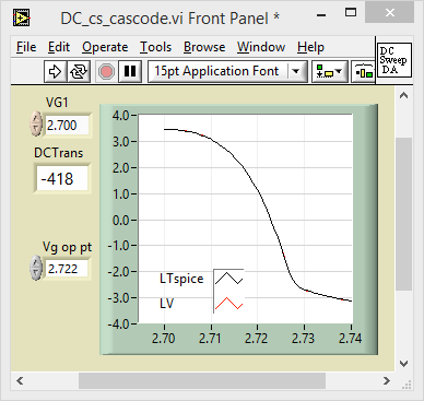
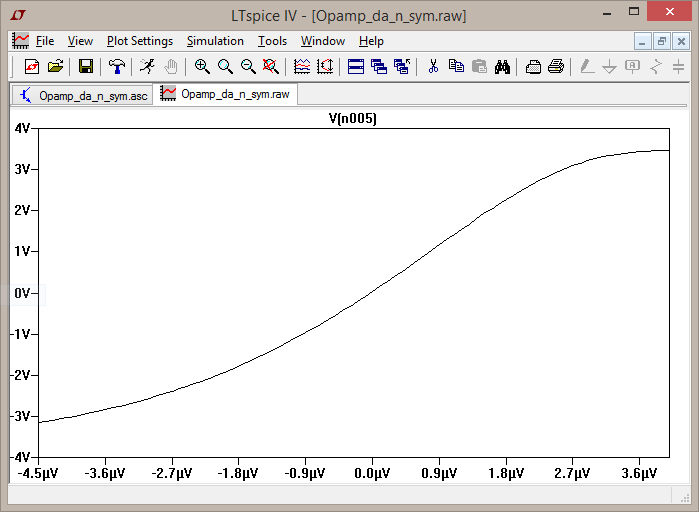
DC Transfer

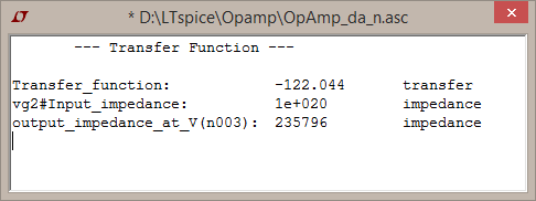
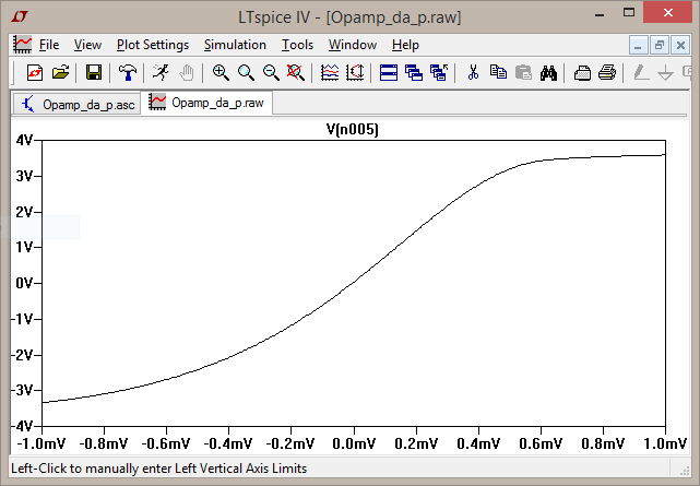
LTspice DC Sweep – Output

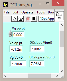
Read Plot data with LabVIEW

DCsweep slope information computed from LTspice DCsweep data.

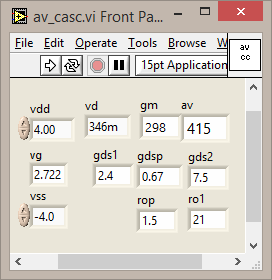
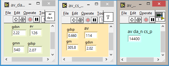
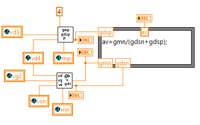
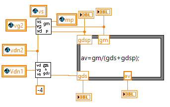
Signal Gain Compute
Diff Amp
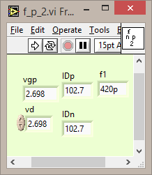
Common-Source

Opamp 2 – PMOS Diffamp Opamp – Includes constant gm reference circuit. Opamp results are the same as with standard reference circuit at a given bias. Diffamp and Common-source gain stages have drain currents as in above circuit. Compare DC characteristics.

DCtransfer

Signal Gain
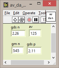
Parameter gdsn in diffamp is high (low output resistance) due to Vds being near saturation and the fact that the NMOS is in the substrate (versus the well). Parameter gm p is greater than gm n (cs) due to 2x relative W. Parameter gm p in above case is close to gm n but has 2 x the gate width in the PMOS.

Diff Amp
Common_Source

LTspice DCsweep
Plot data slopes.

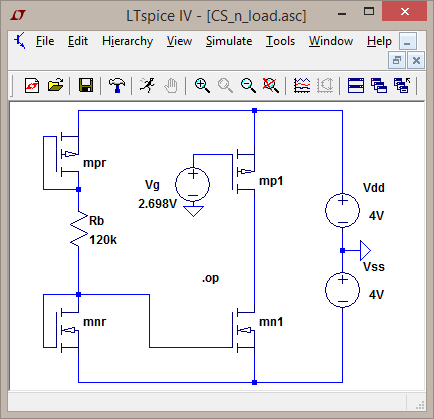
Opamp 3 – NMOS current source diff amp with cascode-load common source. M1 is a common-gate stage with gate signal zero and bias from gate-drain of M4. M2 is a common-source stage with output resistance the input resistance of M1 and DC bias from M3. Gain stages have ID = 100 uA.

DCtransfer
Benefit comes from the fact that the NMOS has the lower output resistance.

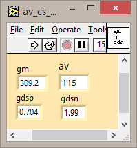
Signal Gain

Cascode-stage gain.
Output resistance from drain of common-gate is 19 megOhms such that gain is approximately open-circuit gain of PMOS Mp1.

Computed slopes from LTspice DCsweep data.

Opamp 4 – Symmetrical output NMOS source diffamp, with symmetrical output.
DCtransfer – Vd2 – Input Diff Amp – Single Ended

DCtransfer

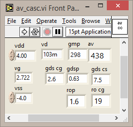
Signal Gain Computation for Input Diffamp Stage – LabVIEW
Note low output resistance of NMOS due to low Vds.

DCsweep – LTspice
Opamp 5 – PMOS Current Source Input Diffamp

DCtransfer – Vd2 – Input diff amp, single ended.

DCtransfer

Signal Gain – Diff Amp

Opamp 6 – Input Diffamp with Folded Cascode Load – Mp1 and Mp2 are in common-gate mode with ac ground at Vgr.

Diff Amp – Single Ended

DCtransfer

Opamp 7 – PMOS Input Diff Amp

Diffamp DCtransfer

DCtransfer

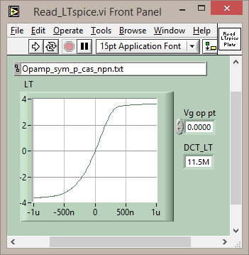
Read LTspice DCsweep – LabVIEW

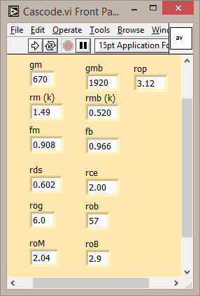
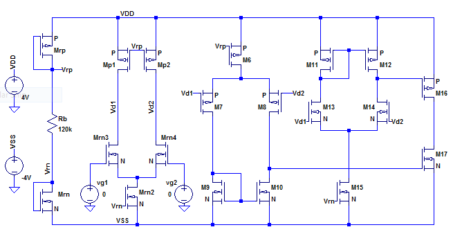
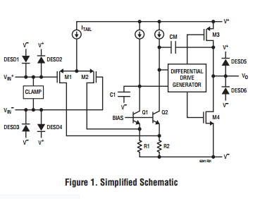
Opamp 8 – Opamp 7 with npn cascode BJT devices.
Input configuration borrowed from LT 6240 opamp.
Read LTspice DCsweep.

Opamp 7 and 8 Comparison
Left column is for NMOS (M4 and M5) and the right column applies to the BJT (Q1 and Q2). Parameter rm in input resistance of common-gate or common base. Parameter fm, fb is portion of diff stage signal drain current which goes to output versus to Rb. Parameters rog and rob are resistances (megOhms) from cascode outputs. Parameters roM and roB are output resistances. Parameter rop is PMOS output resistance (megOhms) (M18 and M19). BJT case produces about 1.4 factor in higher DC transfer.