Estimation of MOSFET Parameters for Circuit-Simulation
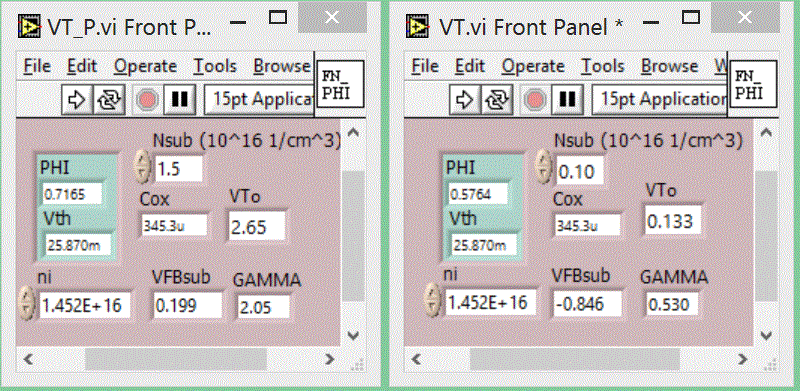
NMOS and PMOS Model Threshold Voltage and GAMMA for Simulator Model (EKV)
No Implant – Neglect Interface Charge
VTO
P-Well – PMOS – NMOS Examples

N- Well PMOS – NMOS Examples

LAMBDA
Level_3
Use Level 3 to generate simulated measured data. Level 3 includes the P-N junction depletion-region function for channel-length modulation, thus, the doping dependence is taken into account. Obtain a curve fit with EKV to obtain LAMBDA. GAMMA and VTO are from the above formulation. KP (mobility) is assigned a typical value.

All Parameters

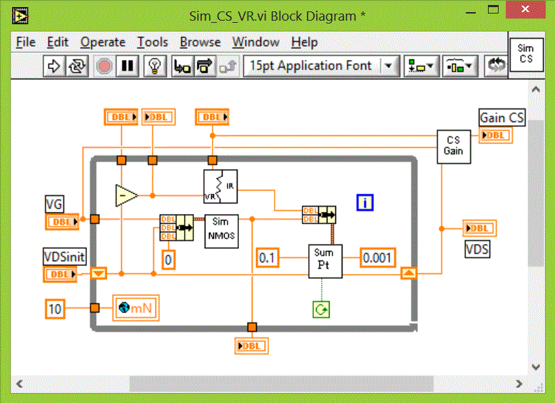
CS with RD Common-Source Simulation with Above Parameters
VG is set for Vo=4 V with VDD=8 V. LAMBDA_N is launched in the background, which runs VT.

Iteration on VDS
VDD-VDS is applied across resistor. Iteration halts when NMOS simulator current and resistor current are equal. The three inputs to the NMOS simulator, top to bottom, are VG, VDS, and VS.

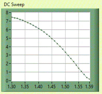
DC Sweep

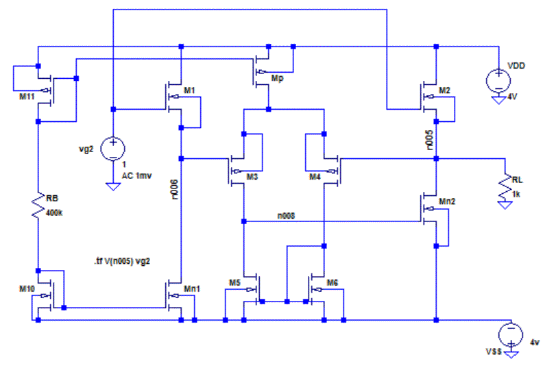
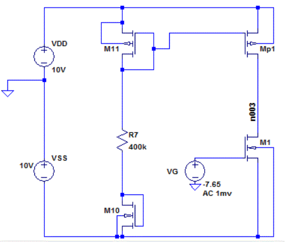
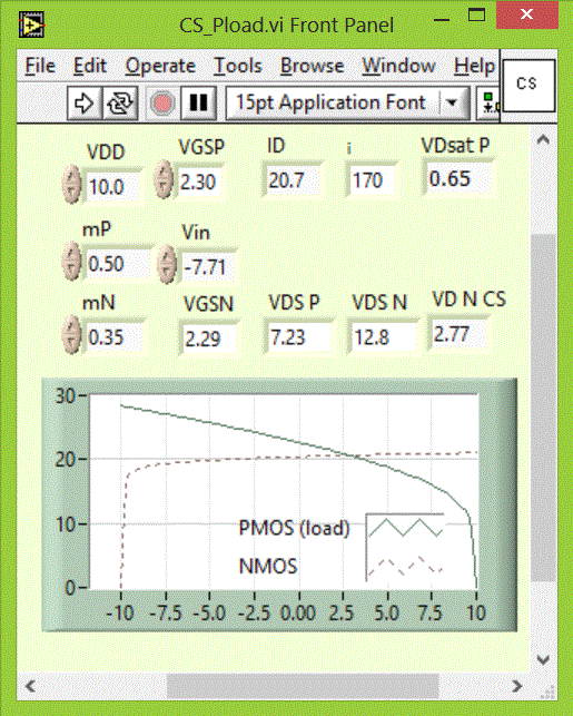
The next circuit is a CS with active (PMOS) load, with circuit as given here. It includes the reference voltage circuit for the PMOS. (LTspice.) The bias current is the same as in the above circuit. The DC transfer is now more than doubled, plus the need for the load resistor is eliminated. The resistor in the bias circuit is external to the integrated circuit.

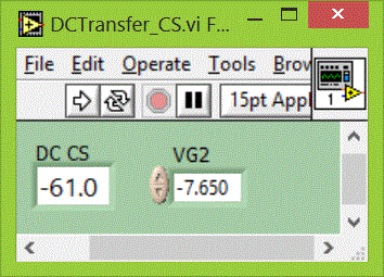
LabVIEW DC Transfer

CS + SF
The buffer stage allows for small loads without diminishing the gain.

DCSweep

CS
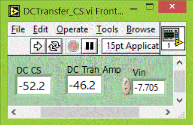
Output has been moved to 2.77 V, to set SF at zero Vo.

DCtransfer
CS gain is reduced at new bias point.

Optimize Gain with Gate Width