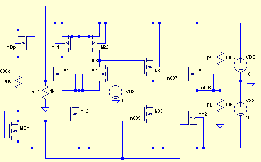
Version II Our amplifier, from LTspice is as follows. Factors affecting gain, bandwidth, and load-current capacity are considered. Simulator is EKV.
Initial design gives the following, from LabVIEW simulator. The gate width is specified in units, mP and mN, with all equal to 1 except for the source-follower output stage and for mP(M3) to balance the output.
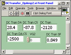
DC Transfer Small-Signal Equivalent

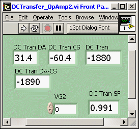
DC Transfer
The bandwidth for this case is 450kHz, from Schematics.
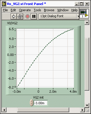
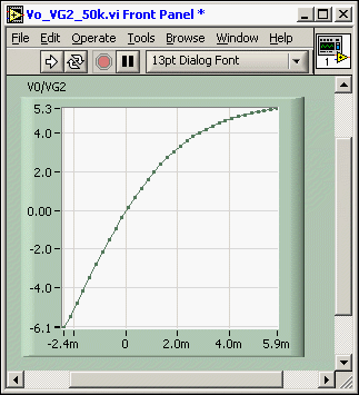
DC sweep for RL=5k, non-inverting.
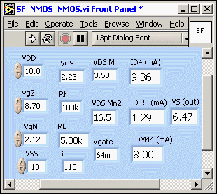
SF output stage at max in above plot. About 9 mA available for load.
Common-source functions versus ID (RB). mP=1.4, mN=1, VDSP=8V, VDSN=12V. DC bias VGSP and VGSN are from amp bias circuit. Load is dominated by PMOS for both stages. ID common-source for above DC Transfer simulation is 30.9 uA.

Set
mN(MS)=0.5,
mN(M1,M2)=4,
nP(M11,M22)=8,
mN(M33)=0.5,
mP(M3)=9.3 for balanced zero output.
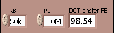
RL=500k. DC Transfer:

Circuit voltages and currents.

New bandwidth, 87 kHz.

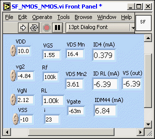
Maximum negative voltage for RL=1k, and ID (RL)=6.4 mA. The load current is supplied by M44 such that VGS4 rises to 1.55 V, the result being a non-unity gain output stage.
Reduce reference current resistor to RB=250 kOhms. Now have 15 mA into 500 Ohm load.

DC sweep for RB=50 k, RL=100 Ohms. Max negative load current is 60 mA.
DC Transfer – Bandwidth=420 kHz
Amp with Negative Feedback
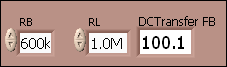
DC Transfer -Ideal Limit = 101

Leave a comment