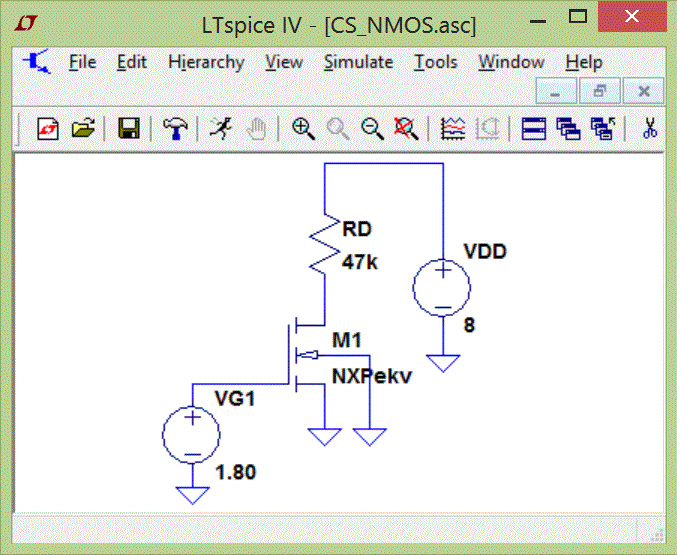
The circuit is constructed for testing from the chip. Both transistors use pins 6, 7, and 8 without body effect and the CS uses 6, 7, and 8 and the SF uses 3, 4, and 5 for the BE case, as would be necessary for the total amp coming from one chip.

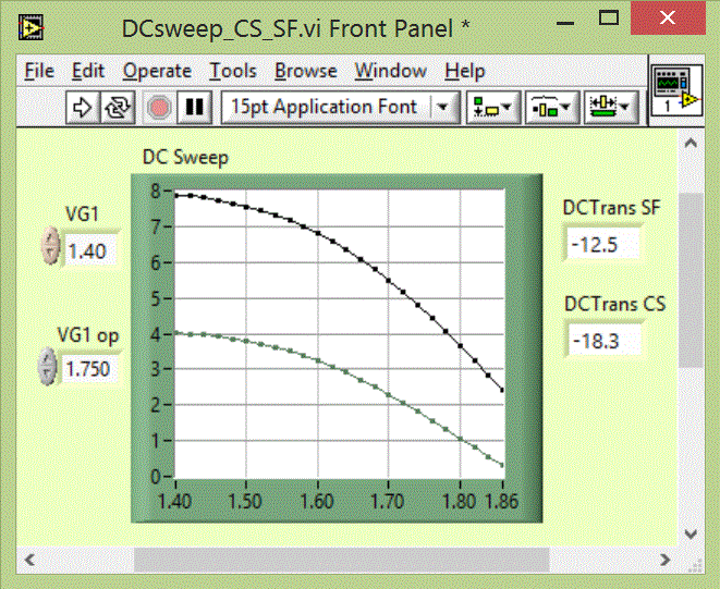
The measured DC sweep for without and with BE are here.

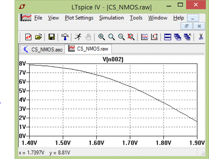
 The Simulations follow,including DCtransfer. The DC transfer is reduced by BE.

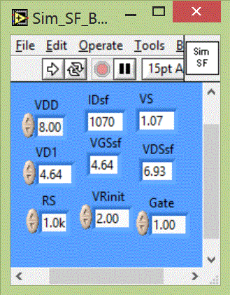
SF simulations at the op pt VG=1.75V are given here. The DC VGS=4.64 volts, due to BE, for the latter case. The op pt ID is 1.7mA for the firsts case, with the 1k load.

The Gate width of the SF NMOS is now made 20 times that of the CS, with the following. The VGS of the SF is now down significantly and the DCtransfer loss across the SF is relatively small.
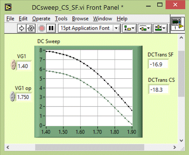
The larger DC output also permits a large bias VGS1, along with an improved DC transfer, as in the following.

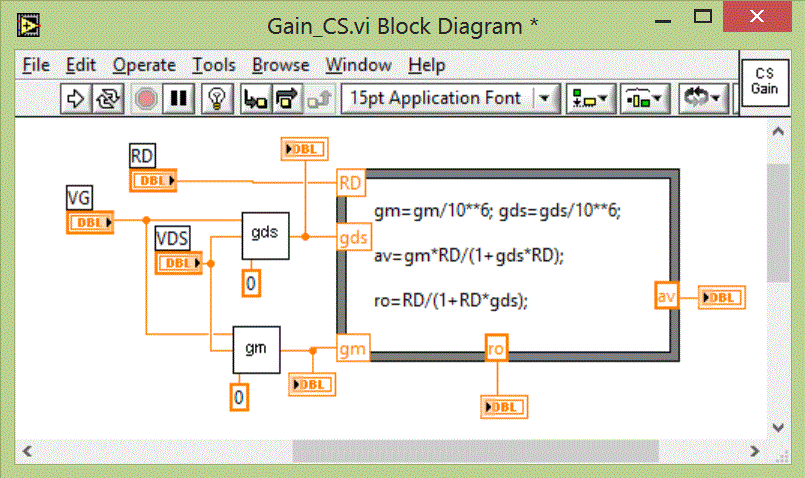
The small-signal gain computation gives the same result for CS stage, as shown here.

DC sweep from LTspice, VD CS.
DCtransfer from Multisim

Multisim DCsweep, VD CS


Leave a comment