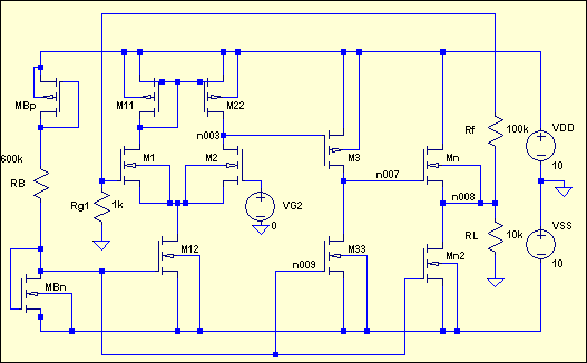
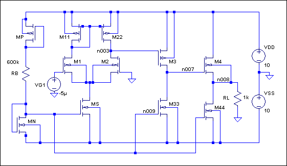
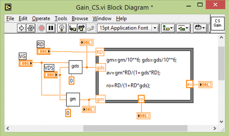
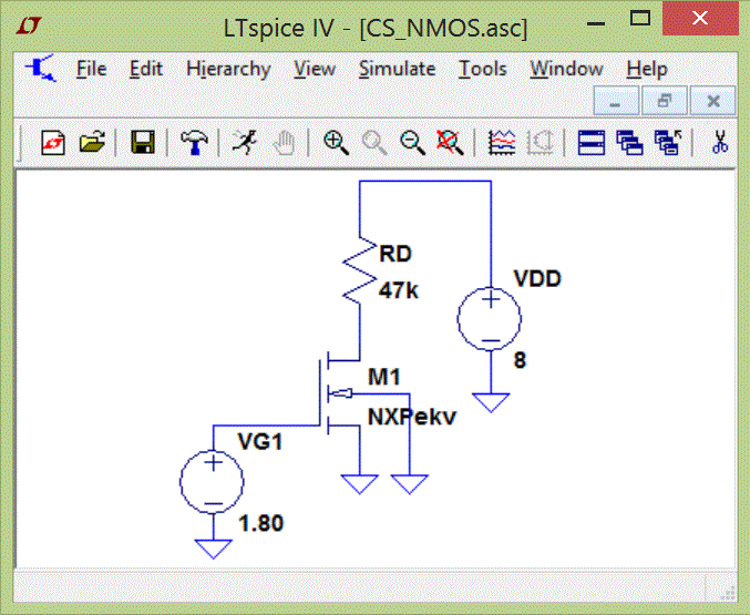
Circuit
Shown is the output segment of the Op Amp with a standard, basic source-follower output stage, along the the common-source stage. The input to the CS is from the DiffAmp stage. This source-follower stage is later compared with the output stage of the TS271. The simulation is EKV and the parameter set is for an N substrate with P well (NMOS). The opposite is compared below.
VTO p = 1.25 V – VTO n = 1.51 V
Common-Source Stage
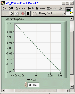
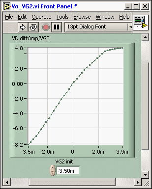
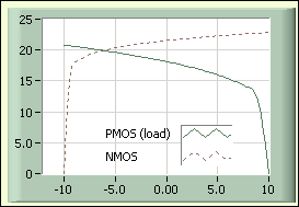
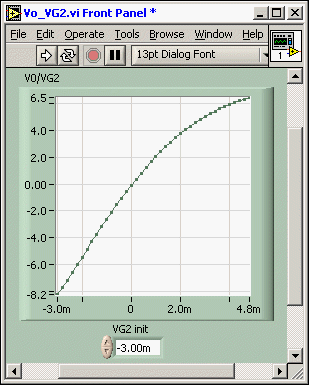
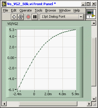
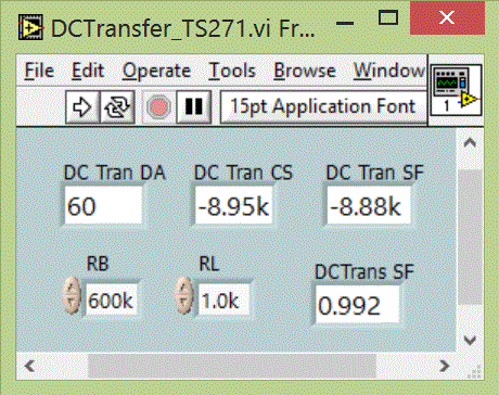
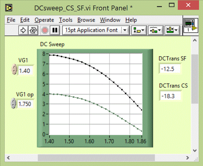
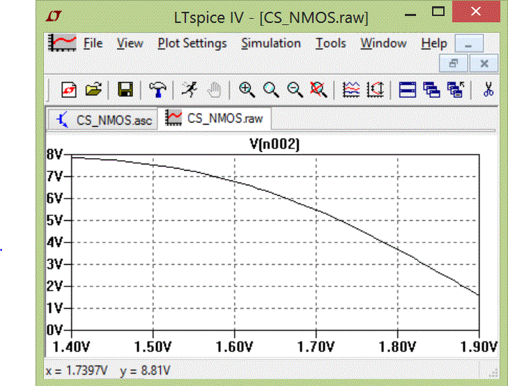
DCsweep – CS Output

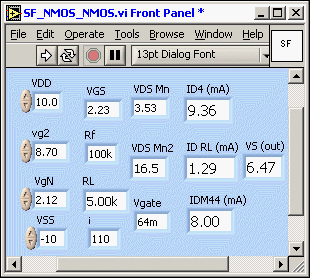
CS Output at the Minimum
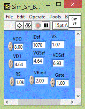
CS Drain Current about 20 uA at Op Pt
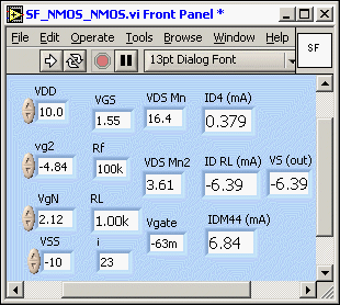
CS Output at Maximum

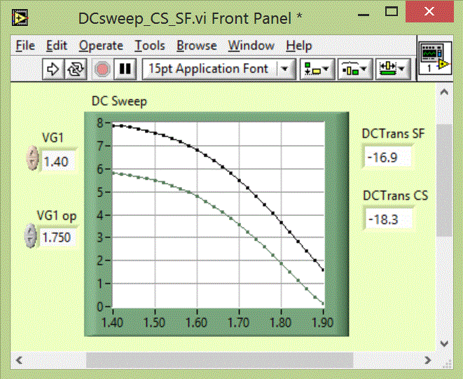
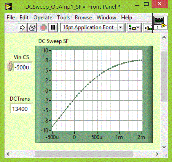
DC Sweep with SF Output
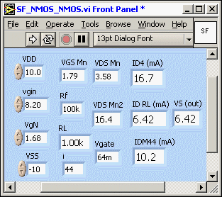
VGS(M2)=2.09 V.
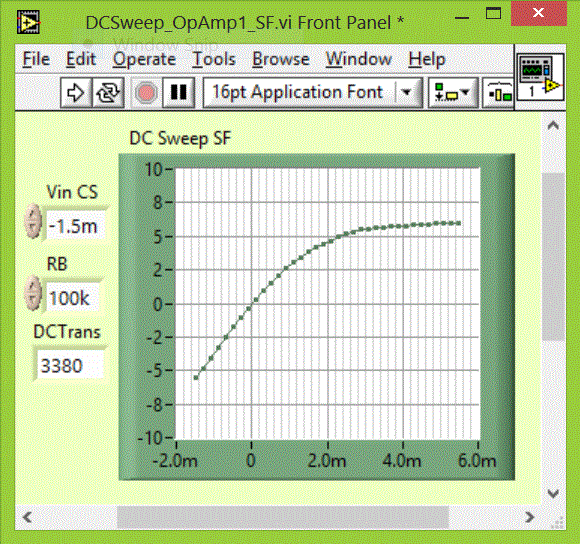
RB=100 k for Larger Output Current
CS at Max Above
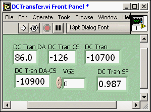
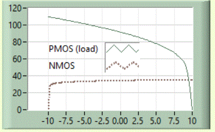
Op Pt CS Drain Current 90 uA. RL=1k for 6 mA output at max. Available output, 12 mA.
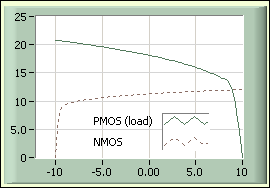
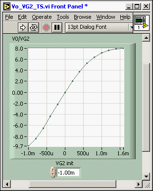
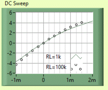
Sweep with and without Load
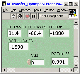
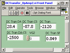
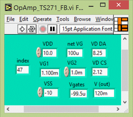
Compare with OpAmp with TS271 Output Stage

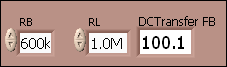
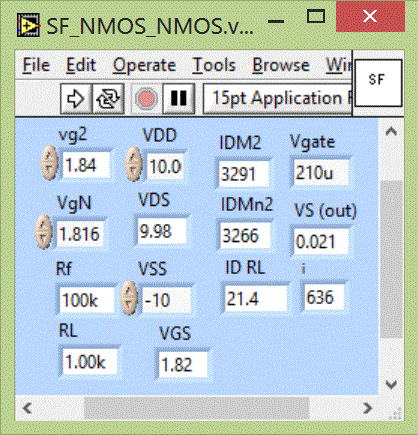
Source Follower Stage for Two Loads and Two Types
Standard SF – 1MEG load -IDM2 about equal to IDMn2

Standard Source Follower – RL=1 k, load current all from increase from M2.
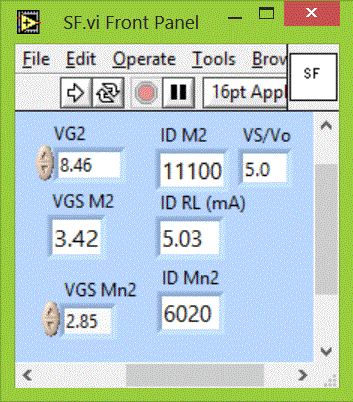
TS271 Output Stage – RL=1MEG – negligible load current.

TS271 Output Stage – ID (M2) essentially unchanged (and thus, VGS(M2)). Feedback circuit reduces VGS (Mn2) to account for approximately 5 mA load current.

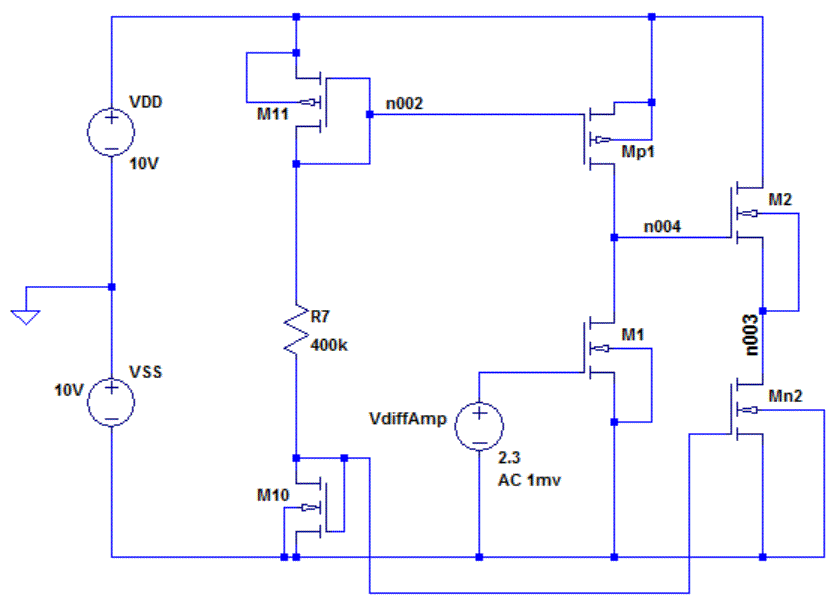
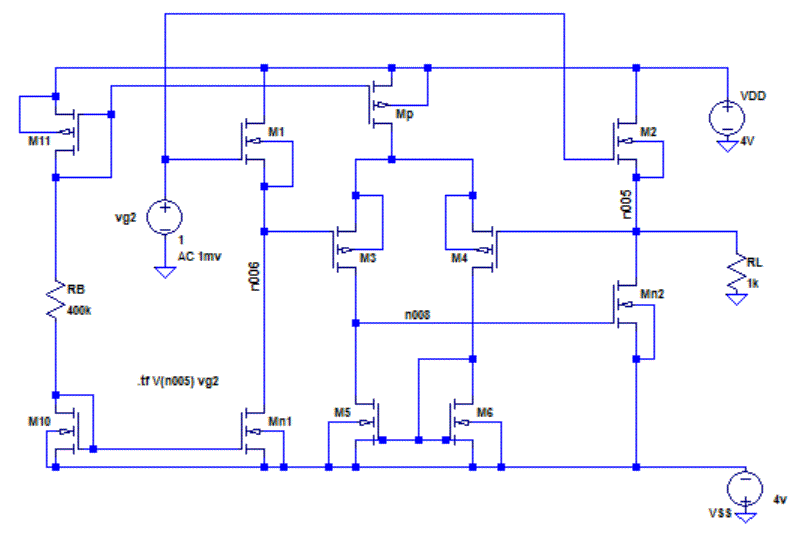
TS271 Output Circuit (LTspice)
Input to Mn2 is drain of M3.
Example 2
N-Well
VTO n=0.133 – V VTO p=2.45 V
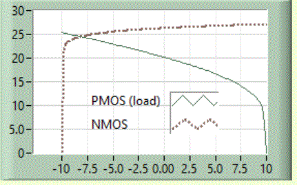
DCsweep – Maximum is now limited by VGS(M3), which pushes VGS(MP) into pre-saturation.

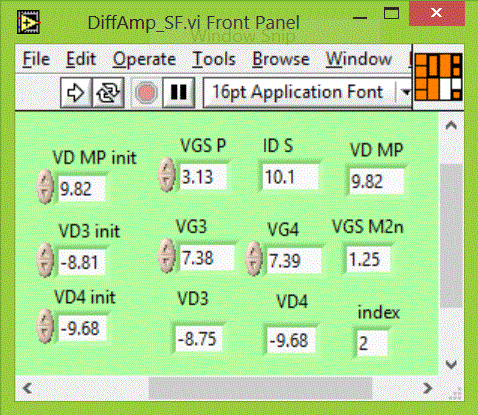
Diffamp of output stage at max above. Note that VD(MP) is at 9.62 V