Kla's Blog

January 25, 2013

MOSFET Amplifier Tutorial

Filed under: Uncategorized — kla @ 8:27 pm

The basic common-source amplifier is given here, from Schematics.

ALLES

Plots of the load resistor and PMOS characteristics are shown here. The PMOS gate voltage is selected to provide an intersection at VD=4 V, for a suitable operating point. The gain will be the transconductance gm divided by the sum of  gds of the transistor, and 1/RD, that is the load conductance. The plots indicate that there exists a somewhat linear range for over plus and minus 2V.

ALLES

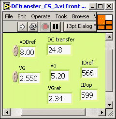
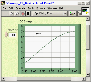
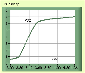
A DC sweep follows. The pre-saturation appears on the right end, and the center confirms the bias point from the above plot. A linear estimate from VG1=2.2 to VG1=2.6 for an increment of VD=3 V predicts a DC transfer of -7.5.

ALLES

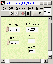
The DC transfer simulator is used to check the results. The DC transfer is the slope over a short range of VG. CS gain is computed as shown below.

ALLES

ALLES

NMOS  case. The gds of the NMOS is superior, as is gm.

ALLES

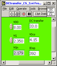
The following is for replacing RD with an NMOS. VGn is adjusted for the same output bias voltage. The slope of the NMOS is much less than for case of RD. The NMOS load is equivalent to a resistor with intercept at a negative VDS value.

ALLES

This circuit, from Schematics, with dual power supplies, is shown here. Note that the gate voltage VGSp is 4-1.65.

ALLES

A DC sweep from Schematics follows, with variable VGn. The bias value, for VD=4 V, agrees with the above plot. The DC transfer is given below. The output resistance is about 37k compared with approximately 10k for the RD case.

ALLES

ALLES

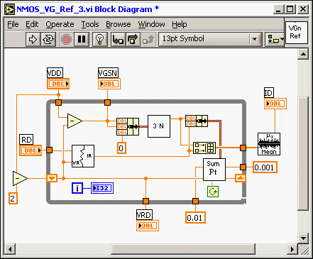
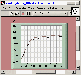
The LabVIEW simulator for the circuit is here.

ALLES

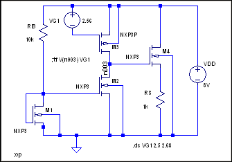
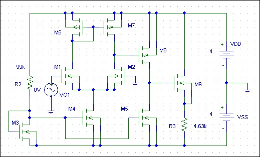
The practical amplifier replaces the DC source with a diode-connected transistor as in the next circuit. The value of R2 is selected to establish the voltage VGn of the above circuit, which is VGS3, with VDS3=VGS3. The DC transfer is the same as in that circuit.

ALLES

The LabVIEW simulator now includes this feature. The voltage VGn here is supplied by the reference circuit.

ALLES

The reference voltage iteration loop is as follows. The iteration is on the resistance voltage, and the loop halts when the current through the resistor is equal to that from the NMOS simulator, 3 N.

ALLES

January 24, 2013

Common-Source Source Follower in Operational Amplifier

Filed under: Uncategorized — kla @ 11:13 pm

Our DC plots for the CS-SF amplifier are, from the last post, as follows. For a differential amplifier application, VSsf should be near 4 volts, or zero for bipolar power supplies. As in the bottom, this is accomplished by increasing the effect gate width of the SF stage, by a factor.

ALLES

ALLES

The CS-SF stages are now incorporated into the operational amplifier, as follows from schematics. The gate dimensions are based on 3 in parallel for most of the devices, with M9 assigned 24. M5 is two and M8 is five. This places the drains of these two at an appropriate DC value to place the source of M9 at near zero. With feedback, the output is forced to zero, and the amp assumes values accordingly.

ALLES

The following is the DC Operational Amp simulator, from LabVIEW. The results agree with Schematics, DC and DC transfer.  The source of the source follower is at 0.8 V.  VDS of the CS is only 0.8 V but this will increase to about 1.6 V with feedback. We note that VD CS – VS SF= 2.37 is consistent with the separation of the two DC plots in the above sweep of the CS-SF amplifier, for the same gate proportions. The diagram below displays the NMOS drain-current reference circuit, the loop for the differential amplifier, the common-source loop and the source-follower loop.

ALLES

ALLES

January 23, 2013

MOSFET Common-Source Source-Follower Amplifier Evaluation with Spice Level 3

Filed under: Uncategorized — kla @ 4:28 pm

The amplifier is constructed for comparison with simulation. The chip is shown here. The NMOS reference and load use pins 3, 4, 5, 6, 7, and 8. The PMOS, on another chip, uses 6, 13, and 14. The source follower is from pins 6, 7, and 8, initially. The goal is to evaluate the DC transfer of the CS stage and the SF stage, and to establish an operating point.  Also, the measured and simulated characteristics (Level 3 Spice) are compared.  The operating current of about 500 uA is within the Level 3 range. Note that VMAX is not used as a parameter. (An example of a case with body effect is discussed below, where the SF uses pins 3, 4, and 5.)

4007

The circuit from LTspice.

ALLES

The measured DC sweep is as follows. To provide the output with a 1.5 V signal range, the bias voltage is set at VGp=2.56 V. The measured DC transfer is computed and displayed.

ALLES

The LabVIEW simulation is as follows. The lower plot gives the amp DC transfer. PMOS parameter ETA is adjusted to improve the DC transfer. The PMOS and NMOS parameter extractions are executed in the background for each simulation.

ALLES

The DC transfer, simulated, for the SF is here. MOSFET follower devices have a relatively poor transfer characteristic. due too a small gm, compared to the BJT (emitter follower). It depends on the load resistor, which is 1k in this case. With body and source connected, there is no body effect.

ALLES

With the PMOS ETA adjustment, a very good fit to the output characteristic is obtained, as shown here.

ALLES

The Sweep above runs the single-point simulator, as shown here.

ALLES

It runs the reference current simulation, the CS simulation, and the SF simulation. Each of these iterate node voltages to match currents, for example, PMOS and NMOS simulators for the CS simulator. The other two match current through a resistor with that from the NMOS simulator.

ALLES

A DC sweep with LTspice produces the following for the drain of the CS stage and SF below. Note that a rough straight-line fit to the lower curve gives about 20.

ALLES

ALLES

Body Effect

Here we evaluate the body effect and the role it plays in reducing the transfer of the SF. It is also a test of the simulator. The SF now uses pins 3, 4 (source), and 5 (VDD). Pin seven is at ground (body reference).

4007

Measured DC voltage are now as given here. The lower output voltage is a function of the increased VGSsf.  Below is the LabVIEW simulation.  At the bottom is the single-point DC transfer, with the transfer function computed again for the bias from above.

ALLES

ALLES

ALLES

Shown  here is the simulated DC transfer for the entire range.

ALLESLTspice DC sweep of the source is here.

ALLES

The new circuit. The DC transfer function from LTspice and AIM spice do not match the results also DC bias is the same. Schematics gives a result matching that of LabVIEW.

ALLES

January 19, 2013

CMOS Simulation with Level 3 Spice – Part 2

Filed under: Uncategorized — kla @ 4:45 pm

In a previous post, VTO was obtained by a data intercept. Here, we will use a slope fit to the Transfer Characteristic (wide range of ID with constant VDS). The comparison is here for the NMOS. VTO now is allowed to vary with the selection of other parameters, and is a reflection of the fact that the actual case departs from the simple case.

ALLES

The simulated CMOS response for three of the available samples is given here.

ALLES

The three parameters, with GAMMA assigned, are shown here. UO is the sum fit to the transfer function, VTO is a slope fit, and KAPPA is a slope fit to the output characteristic. VMAX, ETA, can be assigned.

ALLES

UCRIT= 1M (VMAX=44k) produces the lower output characteristic here (NMOS), with improved pre-sat fit, while the upper is without velocity saturation included (typical of the basic Level 3). Note that this is otherwise not the standard version of Level 3 with VMAX not zero, but rather only includes the affect on UO from velocity saturation.

ALLES

ALLES

Measured and simulation plots of the three samples are here.

ALLES

January 15, 2013

MOSFET Common-Source Amplifier Evaluation with Basic Level 3 Spice

Filed under: Uncategorized — kla @ 4:20 pm

The amplifier from LTspice is as follows. This is stage 2 of our Operational Amplifier. The R1 size places the operating currents at the bottom end of normal Spice 3 application. The parameter extraction is from the following post.

ALLES

The circuit is constructed and a DC sweep is made as follows. A DC transfer is calculated at the given assigned voltage.

ALLES

The single point DC Transfer computer is given here. The result is close to that measured.

ALLES

The LabVIEW simulator gives the following.  AIM Spice, Schematics, and LTspice give the same result. The match is not good at low VGp bias. The simulator output characteristics for the PMOS gate bias at the low end is are plotted (below). It shows that the slope of the PMOS is critical here and affects the DC transfer over the range of the output voltage.

ALLESALLES

The bias resistor is now made R1=4.63k for a reference current as shown here.

ALLES

The new measured DC transfer is as follows, along with the simulated version below. The match is better and the currents are closer to those used in parameter extraction.

ALLES

ALLESThe OC’s for the lowest voltage:

ALLESA DC Transfer from AIM spice.

ALLES

The OC’s exhibit the glitch in the DC transfer, from the PMOS discontinuity into pre-saturation.

ALLES

AIM Spice Net List. LTspice model is used for direct comparison.

ALLES


A comparison is made here for the three devices, from three sources, in a simulation of the circuit. These are old chips and not a reflection of current-day devices, but provide a comparison of devices with different implant conditions. The parameter finders are the same, except for data measured for the specific device, NMOS and PMOS.


NXP. DC transfer 18.8 at VGp=2.88V.

NXP


Device 2. DC transfer 22.0 at VGp=2.40.

ON


Device 3. DC transfer 14.2 at VGp=3.4V.


TI


January 12, 2013

MOSFET Simulation with Basic Level 3 and CMOS Examples

Filed under: Uncategorized — kla @ 9:58 pm

Our basic level 3 simulator, in LabVIEW, appears as follows. All Parameters used in the simulator are given in the front panel (bold).


ALLES


The Diagram:


ALLES


FN_T: Renews all  relevant physical parameters with temperature dependence.


ALLES

FN_PHI 3: Updates all GAMMA (NSUB) information.

ALLES

VDsat: Note that VTO is an extracted parameter.

ALLES

iD:

ALLES

FN_S: This version includes the possibility of velocity saturation, but Vb is set at very large for now.

ALLES

Initially, VT=VTO is found as the intercept in the first equation here,  based on a transfer-function measurement with VDS=2V. VTO is read in as a global variable, to be used elsewhere. With VTO known, the transfer function (array global variable XM1) is simulated as shown below.

GAMMA is a guess value, initially.

ALLES ALLES


(Modified version.)


ALLES ALLES ALLES


A sample resulting fit is shown here, including a plot with the square root of ID. On the right is the data cluster for comparing measured and simulated drain current, as a function of VG1.


ALLES


Shown in the following are fits to output characteristics, grounded source, and computed from the nodes of M2. GAMMA is adjusted for a best slope fit to the latter.


ALLES ALLES


PMOS:


ALLES

Data

Shown here is a data VI. The data array for the transfer function is on the right. The data are defaulted to be used repeatedly. Data can be manually entered into this type of array.

ALLES

The diagram is as follows. XM1 and XM2 are selected from the complete array. The measurement VI is contained in a Case Structure. After data are obtained, the state of the VI is set to False, as given below. Inside the Case Structure is a Local Variable, representing data array (defaulted and save) XF.

ALLES ALLES

A LabVIEW CMOS simulation follows here, based on the results. The Diagram is below. The inside loop iterates on the output voltage to find a NMOS/PMOS current match. The outside loop steps the gate voltage.

ALLES ALLES


From LTspice:


ALLES ALLES

The following is the CMOS response from a different supplier. It appears to have an overdose of implant voltage, as the switching voltage is shifted to a low value. The LabVIEW extractor and simulator provides a simple means of making the assessment.

ALLES

An additional sample is that which appears to have no implant, or possibly the implant is much too deep. The NMOS and PMOS threshold voltage are essentially characteristic of that expected from no implant, and serve to explain why they normally have an implant.

ALLES

A CMOS measurement now gives the following. The PMOS uses pins 6, 13, and 14 and the NMOS, pins 6 (common gate), 7, and 8. The came chip and devices are used for parameter extraction. The bottom plot is measured and simulated with the NXP parameters from above. The measured data are save as a source and re-plotted in the top plot, along with simulated data using new parameters, with an improved fit. The new parameters were obtained with the parameter extraction data being more in the range of the CMOS drain current, i.e., a max of about 600uA. The results are different as Level 3 is not a wide range simulator, but artificial parameters can be be  used for such an application. (This has been replaced with a higher simulation point density for a better comparison.)

ALLES

January 8, 2013

NMOS Cascode Analysis with LabVIEW Level 3 Simulation

Filed under: Uncategorized — kla @ 11:43 pm

Our circuit from LTspice is as follows: (This has been revised. The circuit shown had connected source, body, while computations included the body effect.)

ALLES

The LabVIEW  simulator Front Panel is as given here. The DC information is presented as computed for the given gate voltage. Note that the output signal is in the range of VGS2 and VDS2 is very approximately half of that. ALLES The DC transfer gives the following. LTspice is in agreement as given below. The output resistance is close to the value of the resistor RD. ALLES ALLES The DC Transfer uses the difference between VG1 and plus and minus 10mV. ALLES Cascode loop: Sim L3 is for M1. The details of the M2 circuit are below. The three node-voltage inputs to the NMOS simulator are VG, VDS, and VS. The loop halts when the drain currents from M1 and M2 are close to equal. Sum Pt is a general function used in all of the iterations of our simulators. It produces an off bit when the compared variables are within the number given on the right, 0.001, in this case. The number in the loop, also 0.001 in this case, is the “damping” factor, and is adjusted for maximum rate of convergence.

ALLES ALLES

January 6, 2013

MOSFET Parameter Extraction with LabVIEW for the Operational Amplifier

Filed under: Uncategorized — kla @ 8:58 pm

The LabVIEW simulator (ekv/Bucher, v262) is applied to fitting a simulation to the active-load common-source amplifier  (stage 2) measurement with the goal of simulating the operational amplifier   The emphasis will be for moderate inversion, that is, where the surface potential at the source is approximately equal to PHI. The technique is to compare the measured and simulated data from the common source stage 2, and adjust parameters for a good fit.

 The operational-amplifier circuit from Schematics is here. It consists of a differential stage, a common-source stage, and a source-follower stage.

ALLES

The common-source stage, along with the source-follower stage, is given here, from Schematics. The bias current (M3, M5, and M8) is about 60 uA.

ALLES

The actual circuit uses pins 3, 4, 5, 6, 7, and 8 for the NMOS devices (drains indicated), and, on another chip, pins 13, 14, and 6, for the PMOS. On another chip, the source follower uses pins 6, 7, and 8.

ALLES

A DC measurement sweep and simulation are given here, along with  other results. The parameter extractions are executed in the background while adjusting LETA. The parameter extraction data and circuit are from different chips.

ALLES

Displayed here are the simulated output characteristics at the operating-point PMOS gate voltage.

ALLES

Operational Amplifier

The results are now applied to the operational amplifier. First, it is noted that that reference voltages from M3 and M6 are associated with difference drain currents, that is, ID3 is about twice ID6. Thus, with gate widths the same for all transistors, M5 is in pre-saturation, and VDS5 is about 10mV. Our LabVIEW simulator shows this result, i.e., the drain voltage of the common-source load transistor is -3.90V. The drain voltage of the output of the differential amplifier is 2.18V. We here assume that all devices have 3 gates in parallel, but will set M5 at 2.

ALLES

The LabVIEW DC Transfer computation is as follows. Schematics gives 53.8, -4440, and -3290. Note that this depends on using GAMMA or NSUB in the parameter set, in which case the results are slightly different. This could be a function of the choice of the relative permittivity of silicon. The circuit from LTspice produces 53.2, 4240, and 3140.

ALLES

We test the amplifier in the negative feedback mode, by adding the resistors as shown. The ideal gain is now 11 and Schematics gives 10.95, as expected for an overall gain of about 3000.

ALLES

Create a free website or blog at WordPress.com.